Chapter 1
Introduction to Spice
This chapter introduces electronic circuit simulation using Spice[1], and outlines the basic philosophy of circuit simulation and explains why it has become so important for today's electronic circuit design. We then summarize the capabilities of Spice and the computer conception of electrical and electronic elements and give examples.
Although this chapter is an Introduction to Spice it could just as easily be an Introduction to PSpice. When we make specific reference to Spice by name, our discussion applies equally well to PSpice. However, statements made about PSpice do not, in general, apply to Spice.
1.1 Computer Simulation of Electronic Circuits
Traditionally, electronic circuit design was verified by building prototypes, subjecting the circuit to various stimuli such as input signals, temperature changes, and power supply variations, then measuring its response using appropriate laboratory equipment. Prototype-building is somewhat time-consuming but produces practical experience from which to judge the manufacturability of the design.
The design of an integrated circuit (IC) requires a different approach. Due to the minute dimensions associated with the IC, a breadboarded version of the intended circuit will bear little resemblance to its final form. The parasitic components that are present in an IC are entirely different from the parasitic components present in the breadboard, and signal measurements obtained from the breadboard usually don't provide an accurate representation of the signals appearing on the IC.
Measuring the appropriate signals directly on the IC itself requires extreme mechanical and electrical measurement precision and is limited to specific types of measurements (i.e., it is very difficult to measure currents). Furthermore, an IC implementation does not lend itself easily to circuit modifications which must be made at the IC mask level prior to circuit fabrication. Due to processing delay time, this approach may result in weeks between executing the modification and observing its effect.
Computer programs that simulate the performance of an electronic circuit provide a simple, cost-effective means of confirming the intended operation prior to circuit construction and of verifying new ideas that could lead to improved circuit performance. Such computer programs revolutionized the electronics industry, leading to the development of today's high-density monolithic circuit schemes such as VLSI. Spice, the de-facto industrial standard for computer-aided circuit analysis, was developed in the early 1970s at the University of California, Berkeley. Although other programs for computer-aided circuit analysis exist and are being used by many different electronic design groups, Spice is the most wide-spread. Until recently, it was largely limited to main-frame computers on a time-sharing basis, but today we find various versions of Spice for personal computers (PCs). In general, these programs use algorithms slightly different from Spice's for performing the circuit simulations, but many of them adhere to the same input format description, elevating the Spice input syntax to a computer-like language.
Commercially supported versions of Spice can be considered to be divided into two types: main-frame versions and PC-based versions. Generally, main-frame versions of Spice are intended to be used by sophisticated integrated-circuit designers who require large amounts of computer power to simulate complex circuits. Commercial versions of Spice include HSpice from Meta-Software and IG-Spice from A. B. Associates. PC-based versions of Spice allow circuit simulation to be performed on a low-cost computer system. The version of interest to us in this text is PSpice, from MicroSim Corporation.
Although Spice was originally intended for analyzing integrated circuits, its underlying concepts are general and can apply to any type of network that can be described in terms of a basic set of electrical elements (i.e., resistors, capacitors, inductors, and dependent and independent sources). Today, Spice is often used for such applications as the analysis of high-voltage electrical networks, feedback control systems, and the effect of thermal gradients on electronic networks.
Integrated circuit design usually begins with a set of specifications (e.g., frequency response, step-response, etc.). It is the designer's objective to configure an electronic circuit that satisfies these specifications. This task intrigues most circuit designers because so far computers have not yet acquired enough intelligence for it. The designer must rely on his or her knowledge of electronic circuit design. By using approximate methods of analysis, designs can be configured and quickly analyzed by hand to determine if they have the potential for meeting the proposed specifications.
Once a design is found that might meet the specifications, the designer applies more complex models of device behavior (such as those in Spice). The behavior of the design, as simulated by Spice, is checked against the required specifications. If the circuit fails to meet the specs, the designer can return to a simpler computer model, preferably the one used during the initial design, and identify the reason for the discrepancy. When computer simulation shows that the performance of a circuit is not adequate, the designer who understands the components of the design can systematically alter them to improve performance. (Otherwise, the designer must rely on a brute force hit-or-miss approach---which usually results in a lot of wasted effort and probably no improvement to the circuit.) The design process is depicted in the flow chart in Fig. Fig. 1.1.
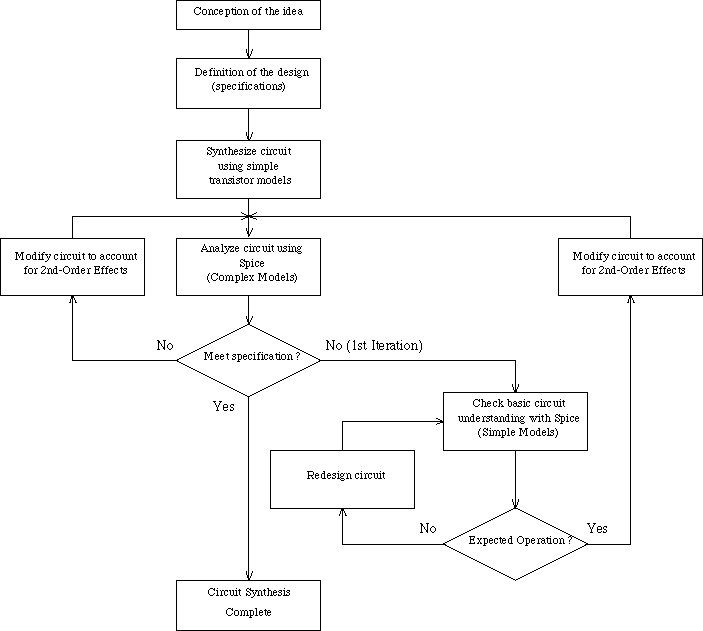
Fig. 1.1: Illustrating the role of circuit simulation in the process of circuit design.
1.2 An Outline of Spice
Spice simulates the behavior of electronic circuits on a digital computer and tries to emulate both the signal generators and measurement equipment such as multimeters, oscilloscopes, curve-tracers and frequency spectrum analyzers. Here we briefly outline the analysis available in Spice and proper way to describe a circuit to Spice. The following description is meant as only an introduction. Later chapters provide more detailed examples.
1.2.1 Types of Analysis Performed by Spice
Spice is a general-purpose circuit simulator capable of performing three main types of analysis---nonlinear DC, nonlinear transient, and linear small-signal AC circuit analysis.
Nonlinear DC analysis or simply DC analysis calculates the behavior of the circuit when a DC voltage or current is applied to it. In most cases, this analysis is performed first. We commonly refer to the results of this analysis as the DC bias or operating-point characteristics.
The Transient Analysis, probably the most important analysis type, computes the voltages and currents in the circuit with respect to time. This analysis is most meaningful when time-varying input signals are applied to the circuit; otherwise this analysis generates results identical to the DC analysis. The third is a small-signal AC analysis. It linearizes the circuit around the DC operating point, then calculates the network variables as function of frequency. This, of course, is equivalent to calculating the sinusoidal steady-state behavior of the circuit, assuming that the signals applied to the network have infinitesimally small amplitudes.
Spice is capable of performing other types of analysis which are generally viewed as special cases of the three main types. We outline them below.
DC Sweep allows a series of DC operating points to be calculated while sweeping or incrementally changing the value of an independent current or voltage source. This analysis is used largely to determine the DC large-signal transfer characteristic. The Transfer Function analysis is related. It computes the small-signal DC gain from a specified input to a specified output (i.e., one of the following: voltage gain, transconductance, transresistance, or current gain), and the corresponding input and output resistance.
In manner similar to DC Sweep, Temperature Analysis allows a series of analyses to be performed while varying the temperature of the circuit. Because the characteristics of many devices depend on temperature, this facility provides a useful tool for investigating the effect of temperature variation on circuit operation. Any of the above main analysis types can be performed in conjunction with Temperature Analysis, thus providing insight into temperature dependencies.
Sensitivity Analysis indicates which components affect circuit performance most critically. (Critical components may require tighter manufacturing tolerances.) There are usually two sensitivity analyses available. The first, DC Sensitivity, is used to compute changes in the DC operation of the circuit resulting from infinitesimally small changes in the values of various circuit components and is available in most, if not all, versions of Spice. The second, Monte Carlo Analysis, performs multiple runs of selected analysis types (DC, AC and transient) using a pre-determined statistical distribution for the values of various components. It is rather complicated and is beyond the scope of this text.
Finally, Noise and Fourier Analysis procedures calculate the dynamic range of a circuit. Noise analysis calculates the noise contribution of each element, injects its effect back into the circuit and calculates its total effect on the output node in a mean-square sense. The Fourier analysis computes the Fourier series coefficients of the circuit's voltages or currents with respect to the period of the input excitation(s).
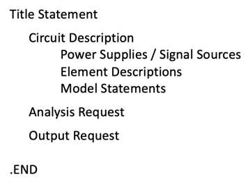
Fig. 1.2: Suggested format for a Spice input file.
1.2.2 Input To Spice
A circuit to be simulated must be described to Spice in a sequence of lines entered via computer terminal into a computer file commonly referred to as the Spice input deck or file. Each line is either a statement describing a single circuit element or a control line setting model parameter, measurement nodes, or analysis types. (Simplified versions will be given later.) The first line in the Spice input deck must be a ``title’’ to identify the output generated by Spice, and the last line must be an ``.END '' statement to indicate an end to the Spice input file. The sequence of the remaining lines is arbitrary. Based on the authors' experience, the format shown in Fig. 1.2 is recommended for the Spice input file's layout, but this arrangement is arbitrary and even we will sometimes deviate from it in examples. Comments sprinkled throughout the file improve readability, identify components of the design, and explain the rationale for the simulation. They are designated by inserting an ``*’’ as the first character of the comment line.
|
Table. 1.1: Scale-factor abbreviations recognized by Spice.
|
Table 1.2: Element dimensions.
|
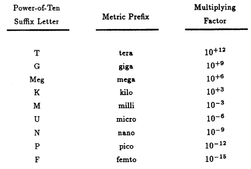
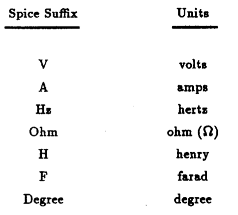
Each statement is of the free-format type; that is, the words used in each statement can be separated by either arbitrary-sized spaces (limited, of course by the line length) or commas, or both. Lines longer than 80 characters (i.e., the screen width), can be continued on the next line by entering a + (plus sign) in the first column of the new line. The original version of Spice was all upper case, but more recent versions make no distinction between upper and lower case. In our future examples we will mix the case type for easy reading. A number can be represented as either an integer or floating point, using either decimal, scientific notation or engineering scale factors. The recognized scale factors are listed in Table 1.1. Not included in this table, but recognized by Spice, is the suffix MIL which is equivalent to 1/1000th of an inch. In addition, the dimensions or units of a given value can also be appended to any element value to clarify its context. The allowed suffix types are listed in Table 1.2.
One word of caution about attaching Farads to a capacitor value. Spice, unfortunately, uses the same letter (F) to denote a scale factor of 10-15 (femto) -- see Table 1.1. One must therefore be careful not to confuse these two suffixes in a Spice input file. Placing a single suffix F on the value of a capacitor indicates that the value of the capacitor is to be expressed in femto-farads not farads. Thus 1 F is 10-15 farads while 1 with no suffix is one farad.
The Spice simulation process begins when we draw a clearly labeled circuit diagram with all nodes distinctly numbered with nonnegative integers between 0 - for the ground node - and 9999. All other components also must be uniquely labeled.
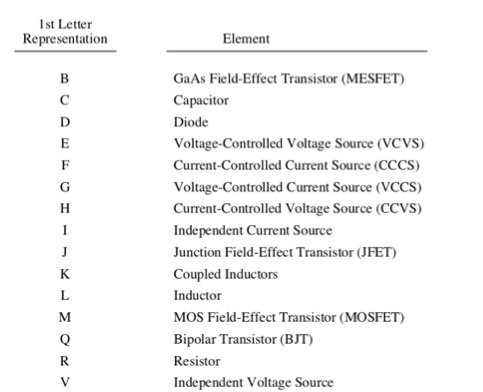
Figure 1.3(a) shows a linear network consisting of various resistors, capacitors and sources (both dependent and independent) with values indicated. In Fig. 1.3(b) each element is assigned a unique name in which the beginning letter (e.g., R, C, E, V) indicates the element type, e.g., R for resistor, D for diode, etc. Table 1.3 lists such key letters available in Spice. For example: the 1 W resistor is assigned the name R1 the load resistor of 10 W is Rload the 2.65 mF capacitor is C1, the voltage-controlled voltage source is E1 and the input sinusoidal voltage source is vi. The ground node is labeled 0, and non-grounded nodes are assigned the numbers 1, 2, and 3.
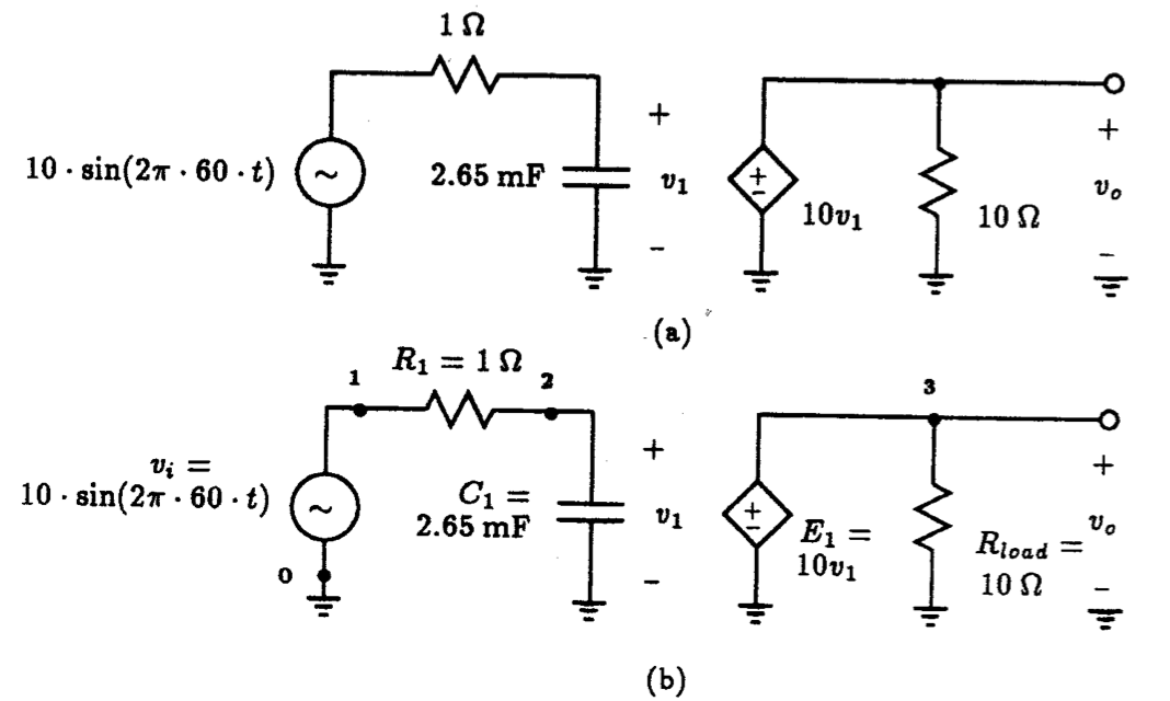
Fig. 1.3: Preparing a network for Spice simulation. (a) Schematic drawing of a linear network. (b) Each element is uniquely labeled, and each node is assigned a positive number with the ground reference point assigned the number 0.
|
Table 1.3: Basic element types in Spice. |
Fig. 1.4: Spice descriptors for passive elements. Fields surrounded by [ ] are Optional. |

The Spice input deck is made up of three major components: a detailed circuit description, analysis requests, and output requests. We now outline the basic syntax of the various commands in these three Spice components.
Circuit Description
Each circuit element is described to Spice by an element statement which contains the element name, the circuit nodes to which it is connected, and its value. Spice knows about four general classes of network elements: passive elements, independent sources, dependent sources, and active devices (i.e., diodes and transistors).
The general Spice syntax for an element description is that the first letter indicates the element type, followed by an alphanumeric name limited to 7 characters which uniquely identifies that element. The information following the element type and name depends on the nature of the element.
Passive Elements: Fig. 1.4 depicts the Spice single-line descriptor statements for an arbitrary resistor, capacitor and inductor. The first field (or set of characters separated by blank spaces) of each statement describes its type and provides a unique name for each element. The next two fields indicate the numbers of the connecting nodes. Although these elements are bilateral, each element is assigned a positive and negative terminal. This convention assigns direction to the current flowing through each device as denoted in Fig. 1.4, but more importantly, it specifies the polarity of the initial conditions as associated with the energy storage devices. The fourth field is used to specify the value of the passive element. Resistance is in Ohms, capacitance in Farads and inductance in Henries. These values are usually positive but can also be assigned a negative value (in which case the elements are not passive). For either the capacitor or inductor, an initial (time-zero) voltage or current condition can be specified in its fifth field (See Fig. 1.4).
For the circuit in Fig. 1.3, the element statements for passive elements R1, C1 and Rload would appear in the Spice deck:
|
R1 1 2 1Ohm C1 2 0 2.65mF Rload 3 0 10Ohm
|
For easy reading, we have attached the dimensions of each element on the end of each parameter value.
|
Fig. 1.5: Independent sources and their Spice descriptions. Also shown is the analysis type for which it is normally used. One exception is for DC sources which are commonly used to set bias conditions in all types of circuits.
|
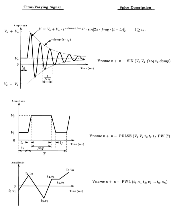
Fig. 1.6: Various time-varying signals available in Spice and the corresponding element statements. Top curve: damped sinusoid; Middle curve: periodic pulse waveform; Bottom curve: piecewise linear waveform. |
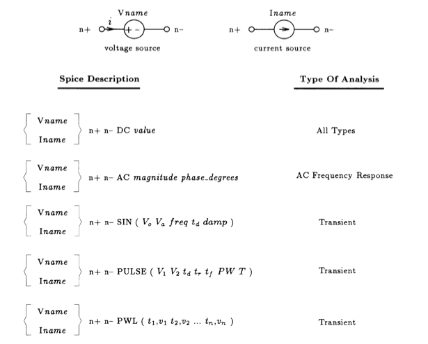
Independent Sources: There are three types of independent sources that can be described to Spice: a DC source, a frequency-swept AC generator, and various types of time-varying signal generators. The independent signal associated with any one source can be either voltage or current. Fig. 1.5 gives a shortened summary of the description of these various sources with the kind of analysis that would be most appropriate for the source type.
With regards to the Spice description of each of these signal sources, the first field begins with the letter V or I, depending on whether it is a voltage or a current source, respectively, followed by a unique 7-character name. The next two fields describe the nodes to which the source is connected to the rest of the network. It is important to respect the order of the nodes because of the signal polarity associated with the source. For example, in the case of a voltage source, the first node is connected to the positive side and the second node to the negative side. As far as the polarity (sign) of the current through a voltage source is concerned, the convention in Spice is as follows: Current flowing into the positive terminal of the source is taken as positive. In the case of a current source, a positive current is pulled from the positive node (n+) and returned to the negative node (n-). The next field specifies the nature of the signal source, i.e. DC, AC or time varying. The remaining fields are then used to specify the characteristics of the signal waveform generated by the particular source. The subsequent signal level parameters associated with the DC and AC sources should be obvious from the Spice descriptions listed in Fig. 1.5. The signal level of the DC source is specified by the field labeled value. The peak amplitude and the phase (in degrees) of the AC source are simply specified in the fields labeled magnitude and phase_degrees, respectively. If the field labeled by phase_degrees is left blank, Spice will assume that the phase is zero.
In addition to DC and AC sources, one can also describe several different types of time-varying signal sources as listed in Fig. 1.5. Included in this list are element statements describing a sinusoidal signal (denoted by the SIN flag), a periodic pulse signal (PULSE) and an arbitrary waveform consisting of piece-wise linear segments (PWL). Obviously, due to the time-varying nature of these signals, these sources can only be used in transient analysis studies. The syntax of these time-varying sources is more complex than that for the DC or AC sources described above, so to simplify matters, we list in Fig. 1.6, the corresponding waveform with the appropriate signal-determining parameters superimposed on each waveform. Although we express these waveforms in terms of voltage, it should be readily apparent that similar waveforms can be described for current sources.
For the circuit example of Fig. 1.3, the input sinusoidal voltage source vI described by 10 sin (2p 60 t) would have the following Spice description:
Vi 1 0 SIN ( 0V 10V 60Hz 0 0 ).
In many cases, the delay time td and the damping factor damp are both zero, so we commonly shorten the above Spice statement to:
Vi 1 0 SIN ( 0V 10V 60Hz ).
This is acceptable to Spice.
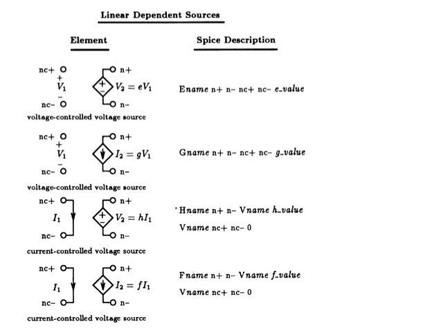
Fig. 1.7: Linear dependent sources. Notice that the CCVS and the CCCS are both specified using two Spice statements, unlike the other two dependent sources.
Linear Dependent Sources: Spice knows about four dependent sources: voltage-controlled voltage source (VCVS), voltage-controlled current source (VCCS), current-controlled voltage source (CCVS) and current-controlled current source (CCCS). These can be either linear or nonlinear, but here we are concerned only with the linear ones. Fig. 1.7 depicts all four sources with the relationship between their input and output variables made clear and also shows the statement used to describe the element to Spice. The name of each dependent source begins with a unique letter (i.e., E, G, H and F) followed by a unique 7-character name exactly like the passive elements described above.
Each dependent source is a two-port network with either the voltage or current at one port (terminals denoted as n+ and n--) controlled by the voltage or current at the other port (terminals denoted as nc+ and nc- ). For the voltage-controlled dependent source, the controlling voltage is derived directly from the network node voltages. A current-controlled source, however, must sense a current through a short circuit that is described to Spice using a zero-valued voltage source, i.e., Vname nc+ nc- 0. This means a current-controlled source requires two statements where a voltage-controlled source needs only one -- an aspect to keep in mind when working with current-controlled dependent sources.
The gain factor associated with the input and output variables is specified in the field labeled value and its dimensions will depend on the type of the dependent source. For example, the voltage-controlled voltage source in the circuit of Fig. 1.3 can be described to Spice as follows:
E1 3 0 2 0 10.
Active Devices: The real computational strength of Spice lies in its ability to simulate the behavior of various types of active or electronic devices such as diodes, bipolar transistors, and field-effect transistors. More recent versions of Spice have been extended to include gallium arsenide transistors.
Active devices are described to Spice in much the same manner as electrical elements: a statement indicating the device type and name followed by the nodes by which it is connected to the rest of the network. The subsequent fields refer to a specific model statement found on another line of the Spice input deck. The model then contains the parameters of the device and the nature of the device model, e.g., npn bipolar transistor. Most active device models are quite sophisticated and consist of many parameters, so this approach has the advantage that more than one device can reference the same model, simplifying data entry to the Spice input file. We defer detailed discussion on active devices until Chapter 3 on diode circuits.
Analysis Requests
Once a circuit is described to Spice via an input file, we must specify the analyses required for our simulation. We have three main choices: DC operating-point, AC frequency response, and transient response. Table 1.4 shows their syntax plus that of the DC sweep command. Notice that each of these commands begins with a dot ``. '' , which tells Spice that the line is a command line requesting action, not part of the circuit description.
The command requesting a DC operating point calculation is .OP and it includes finding all the DC node voltages and currents, and the power dissipation of all voltage sources (both dependent and independent). The .OP command automatically prints the calculation results in the output file.
In general, to determine a circuit's DC transfer characteristic, we need to vary the level of some DC source. We could run repeated. OP commands, but Spice provides a DC Sweep command (.DC) that performs this calculation automatically. The syntax of this command is: the name of the DC source to be varied ( source_name) beginning at the value marked by start_value and increased or decreased in steps of step_value until the value stop_value is reached. We can also vary the temperature of the circuit by replacing the name of the source in the field labeled source_name by TEMP.
|
Table 1.4: Main analysis commands.
|
Table 1.5: Spice output requests.
|
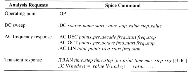
With the AC frequency response command (.AC), Spice performs a linear small-signal frequency response analysis. It automatically calculates the DC operating point of the circuit, thereby establishing the small-signal equivalent circuit of all nonlinear elements. The linear small-signal equivalent circuit is then analyzed at frequencies beginning at freq_start and ending at freq_stop. Points in between are either spaced logarithmically by decade (DEC) or octave (OCT). The number of points in a given frequency interval is specified by points_per_decade or points_per_octave. We can specify a linear frequency sweep (LIN) and the total number of points in it by total_points. We usually use a linear frequency sweep when the bandwidth of interest is narrow, and a logarithmic sweep when the bandwidth is large.
Finally, with the transient response command (.TRAN), Spice computes the network variables as a function of time over a specified time interval. The time interval begins at time t=0 and proceeds in linear steps of time_step seconds until time_stop seconds is reached. Although all transient analysis must begin at t=0, we have the option of delaying the printing or plotting of the output results by specifying the no_print_time in the third field enclosed by the square brackets. This is a convenient way of skipping over the transient response of a network and viewing only its steady-state response. In order to have Spice avoid skipping over important waveform details within the time interval specified by time_step, the field designated by max_step_size should be chosen to be less than or equal to the time_step. The origins of max_step_size is rather involved and interested readers should consult the PSpice Users' Manual. For most, if not all examples of this text, we chose the max_step_size equal to the time_step.
Prior to the start of any transient analysis, Spice must determine the initial values of the circuit variables, usually from a DC analysis of the circuit. If the optional UIC (use initial conditions) parameter is specified on the .TRAN statement, then Spice will skip the DC bias calculation and instead use only the ``IC='' information supplied on each capacitor or inductor statement (see Fig. 1.4). All elements without an ``IC='' specification are assumed to have an initial condition of zero.
Initial conditions can also be set using an .IC command which clamps specific nodes of the circuit at the user-specified voltage levels during the DC bias calculation. This DC solution is then used as the initial conditions for the transient analysis. The syntax of the .IC statement is listed under the .TRAN command in Table 1.4. Note that this command is not used with the UIC flag of the transient analysis command.
Spice can perform many variations of the above-mentioned analysis, as mentioned previously. However, it is felt that at this time introducing these additional commands would only burden our readers with details that will not be used until later chapters of this text. Therefore, we shall defer discussion of these additional commands until a more convenient time.
Output Requests
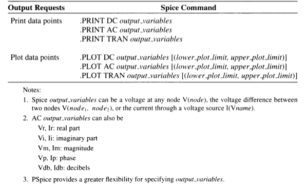
Circuit simulation produces a lot of data, and it would be impractical to pass all of it on to the user. Instead, Spice provides display features that enables us to specify which network variables we want to see and the best format for them. This is much like placing a measurement probe at the node of interest. Table 1.5 lists the syntax of print and plot formats.
The .PRINT command prints out variables in tabular form as a function of the independent variable associated with the analysis. With it, we must also specify the analysis (i.e., DC, AC, or TRAN) for which the specified outputs are desired. Next, we specify a list of voltage or current variables (denoted as output_variables). Generally, a voltage variable is specified as the voltage difference between two nodes, say node_1 and node_2, as V(node_1, node_2). When one of the nodes is omitted, it is assumed to be the ground node (0).
Spice allows only those currents flowing through independent voltage sources to be observed. Such a current would be specified by I(Vname) where Vname is the name of the independent voltage source through which the current is flowing. If we wish to observe a particular branch current without a voltage source, then we add a zero-valued voltage source in series with this branch and request that the current flowing through this source be printed or plotted.
For a DC analysis, the variables printed are the network node voltages or branch currents computed as a function of a particular DC source in the network.
For an AC analysis, the output variables are sinusoidal or phasor quantities as a function of frequency and are represented by complex numbers. Spice accesses these results in the form of real and imaginary numbers or in magnitude and phase form. Magnitude can also be expressed in terms of dBs when convenient. To access a specific variable type, Table 1.5 shows how a suffix is appended to the letter V or I.
The results of a TRAN analysis are the network node voltages or branch currents computed as a function of time.
Spice's graphical feature generates a simple line plot from the list of output variables as a function the independent variable. The syntax for the plot command is identical to that of the print command and .PRINT is replaced by .PLOT. The range of the y axis given by (lower_plot_limit, upper_plot_limit) can be specified as an optional field on the .PLOT command line. (See Table 1.5.)
There are no restrictions on the number of .PRINT or .PLOT commands that can be specified in the Spice input file. This is a convenient way of controlling the number of data columns appearing in the output file.
A Simple Example
For the simple circuit of Fig. 1.3 let us create a Spice input file that would be used to compute the transient response of this circuit for 3 periods of a 10 V, 60 Hz sinusoidal input signal. The Spice input file for this circuit would appear:
|
Transient Response Of A Linear Network
** Circuit Description ** * input signal source Vi 1 0 SIN ( 0V 10V 60Hz ) * linear network R1 1 2 1Ohm C1 2 0 2.65mF Rload 3 0 10Ohm E1 3 0 2 0 10
** Analysis Request ** * compute transient response of circuit over three full * periods (50 ms) of the 60 Hz sine-wave input with a 1 ms * sampling interval .TRAN 1ms 50ms 0ms 1ms
** Output Request ** * print the output and input time-varying waveforms .PRINT TRAN V(3) V(1) * plot the output and input time-varying waveforms * set the range of the y-axis between -100 and +100 V .PLOT TRAN V(3) V(1) (-100,+100)
* indicate end of Spice deck .end
|
The first line begins with the title: ``Transient Response Of A Linear Network,'' followed by a circuit description, analysis request and several output request statements. The final statement is an .END statement. Comments are sprinkled throughout this file to improve its readability. The transient analysis statement,
.TRAN 1ms 50ms 0ms 1ms
is a request to compute the transient behavior of this circuit over a 50 ms interval using a 1 ms time step. The results of the analysis are to be stored in resident memory beginning at time $t=0$ and will later be available for printing or plotting. The last field specifies that the maximum step size is to be limited to 1 ms, the same value as the time step. Finally, to observe the output response behavior, we request that the voltage at the output (node 3) and the voltage appearing across the input terminal (node 1) be both printed and plotted and that the two node voltages be plotted on the same graph with the y-axis having a range of -100 to +100 V.
1.2.3 Output from Spice
Once the Spice input file is complete, the Spice computer program is executed with reference to this file, and the results will be found in the Spice output file. We can examine the contents of this file for the results of the different analyses requested in the input file. If other analysis is needed, we must alter the element statements or add additional analysis commands and re-execute the Spice program until we have all the information we require.
For our example, the results found in Spice output file appear:
|
******* 11/19/91 ******* Student PSpice (Dec. 1987) ******* 10:24:00 *******
Transient Response Of A Linear Network
**** CIRCUIT DESCRIPTION
*****************************************************************************
** Circuit Description ** * input signal source Vi 1 0 SIN ( 0V 10V 60Hz ) * linear network R1 1 2 1Ohm C1 2 0 2.65mF Rload 3 0 10Ohm E1 3 0 2 0 10
** Analysis Request ** * compute transient response of circuit over three full * periods (50 ms) of the 60 Hz sine-wave input with a 1 ms * sampling interval .TRAN 1ms 50ms 0ms 1ms
** Output Request ** * print the output and input time-varying waveforms .PRINT TRAN V(3) V(1) * plot the output and input time-varying waveforms * set the range of the y-axis between -100 and +100 V .PLOT TRAN V(3) V(1) (-100,+100)
* indicate end of Spice deck .end
******* 11/19/91 ******* Student PSpice (Dec. 1987) ******* 10:24:00 *******
Transient Response Of A Linear Network
**** INITIAL TRANSIENT SOLUTION TEMPERATURE = 27.000 DEG C
*****************************************************************************
NODE VOLTAGE NODE VOLTAGE NODE VOLTAGE NODE VOLTAGE
( 1) 0.0000 ( 2) 0.0000 ( 3) 0.0000
VOLTAGE SOURCE CURRENTS NAME CURRENT
Vi 0.000E+00
TOTAL POWER DISSIPATION 0.00E+00 WATTS
Transient Response Of A Linear Network
**** TRANSIENT ANALYSIS TEMPERATURE = 27.000 DEG C
*****************************************************************************
TIME V(3) V(1)
0.000E+00 0.000E+00 0.000E+00 1.000E-03 6.504E+00 3.652E+00 2.000E-03 2.120E+01 6.745E+00 3.000E-03 3.923E+01 8.920E+00 4.000E-03 5.645E+01 9.842E+00 5.000E-03 6.896E+01 9.382E+00 6.000E-03 7.398E+01 7.604E+00 7.000E-03 7.010E+01 4.758E+00 8.000E-03 5.739E+01 1.244E+00 9.000E-03 3.731E+01 -2.445E+00 1.000E-02 1.247E+01 -5.790E+00 1.100E-02 -1.381E+01 -8.322E+00 1.200E-02 -3.792E+01 -9.686E+00 1.300E-02 -5.657E+01 -9.689E+00 1.400E-02 -6.716E+01 -8.331E+00 1.500E-02 -6.825E+01 -5.803E+00 1.600E-02 -5.971E+01 -2.460E+00 1.700E-02 -4.276E+01 1.228E+00 1.800E-02 -1.977E+01 4.744E+00 1.900E-02 6.007E+00 7.594E+00 2.000E-02 3.095E+01 9.377E+00 2.100E-02 5.155E+01 9.843E+00 2.200E-02 6.492E+01 8.927E+00 2.300E-02 6.917E+01 6.757E+00 2.400E-02 6.371E+01 3.638E+00 2.500E-02 4.931E+01 8.124E-03 2.600E-02 2.798E+01 -3.623E+00 2.700E-02 2.716E+00 -6.745E+00 2.800E-02 -2.292E+01 -8.920E+00 2.900E-02 -4.535E+01 -9.842E+00 3.000E-02 -6.140E+01 -9.382E+00 3.100E-02 -6.883E+01 -7.604E+00 3.200E-02 -6.659E+01 -4.758E+00 3.300E-02 -5.500E+01 -1.244E+00 3.400E-02 -3.568E+01 2.445E+00 3.500E-02 -1.136E+01 5.790E+00 3.600E-02 1.456E+01 8.322E+00 3.700E-02 3.844E+01 9.686E+00 3.800E-02 5.692E+01 9.689E+00 3.900E-02 6.740E+01 8.331E+00 4.000E-02 6.842E+01 5.803E+00 4.100E-02 5.983E+01 2.460E+00 4.200E-02 4.283E+01 -1.228E+00 4.300E-02 1.982E+01 -4.744E+00 4.400E-02 -5.972E+00 -7.594E+00 4.500E-02 -3.093E+01 -9.377E+00 4.600E-02 -5.154E+01 -9.843E+00 4.700E-02 -6.491E+01 -8.927E+00 4.800E-02 -6.917E+01 -6.757E+00 4.900E-02 -6.371E+01 -3.638E+00 5.000E-02 -4.965E+01 -2.800E-06
******* 11/19/91 ******* Student PSpice (Dec. 1987) ******* 10:24:00 *******
******* 11/19/91 ******* Student PSpice (Dec. 1987) ******* 10:24:00 *******
Transient Response Of A Linear Network
**** TRANSIENT ANALYSIS TEMPERATURE = 27.000 DEG C
*****************************************************************************
LEGEND:
*: V(3) +: V(1)
TIME V(3) (*+)--------- -1.0000E+02 -5.0000E+01 0.0000E+00 5.0000E+01 1.0000E+02 _ _ _ _ _ _ _ _ _ _ _ _ _ _ _ _ _ _ _ _ _ _ _ _ _ _ _ 0.000E+00 0.000E+00 . . X . . 1.000E-03 6.504E+00 . . .+* . . 2.000E-03 2.120E+01 . . . + * . . 3.000E-03 3.923E+01 . . . + * . . 4.000E-03 5.645E+01 . . . + . * . 5.000E-03 6.896E+01 . . . + . * . 6.000E-03 7.398E+01 . . . + . * . 7.000E-03 7.010E+01 . . .+ . * . 8.000E-03 5.739E+01 . . + . * . 9.000E-03 3.731E+01 . . +. * . . 1.000E-02 1.247E+01 . . + . * . . 1.100E-02 -1.381E+01 . . * + . . . 1.200E-02 -3.792E+01 . . * + . . . 1.300E-02 -5.657E+01 . * . + . . . 1.400E-02 -6.716E+01 . * . + . . . 1.500E-02 -6.825E+01 . * . + . . . 1.600E-02 -5.971E+01 . * . +. . . 1.700E-02 -4.276E+01 . . * + . . 1.800E-02 -1.977E+01 . . * .+ . . 1.900E-02 6.007E+00 . . . X . . 2.000E-02 3.095E+01 . . . + * . . 2.100E-02 5.155E+01 . . . + * . 2.200E-02 6.492E+01 . . . + . * . 2.300E-02 6.917E+01 . . . + . * . 2.400E-02 6.371E+01 . . .+ . * . 2.500E-02 4.931E+01 . . + * . 2.600E-02 2.798E+01 . . +. * . . 2.700E-02 2.716E+00 . . + .* . . 2.800E-02 -2.292E+01 . . * + . . . 2.900E-02 -4.535E+01 . .* + . . . 3.000E-02 -6.140E+01 . * . + . . . 3.100E-02 -6.883E+01 . * . + . . . 3.200E-02 -6.659E+01 . * . +. . . 3.300E-02 -5.500E+01 . *. + . . 3.400E-02 -3.568E+01 . . * .+ . . 3.500E-02 -1.136E+01 . . * . + . . 3.600E-02 1.456E+01 . . . + * . . 3.700E-02 3.844E+01 . . . + * . . 3.800E-02 5.692E+01 . . . + . * . 3.900E-02 6.740E+01 . . . + . * . 4.000E-02 6.842E+01 . . . + . * . 4.100E-02 5.983E+01 . . .+ . * . 4.200E-02 4.283E+01 . . + * . . 4.300E-02 1.982E+01 . . +. * . . 4.400E-02 -5.972E+00 . . X . . . 4.500E-02 -3.093E+01 . . * + . . . 4.600E-02 -5.154E+01 . * + . . . 4.700E-02 -6.491E+01 . * . + . . . 4.800E-02 -6.917E+01 . * . + . . . 4.900E-02 -6.371E+01 . * . +. . . 5.000E-02 -4.965E+01 . * + . . - - - - - - - - - - - - - - - - - - - - - - - - - - -
JOB CONCLUDED
TOTAL JOB TIME 5.82
|
The output file from Spice contains: (1) a replica of the Spice input file or circuit description, (2) the initial conditions for the transient analysis, (3) the results of the transient analysis in tabular form generated by the .PRINT command, and (4) a graphical plot of the transient results produced by the .PLOT command. The output waveform (V(3)), denoted by star-signs (*), almost completes three periods of oscillation, and lags behind the input voltage waveform (V(1)), denoted by plus-signs (+), by about 2 ms or 45 degrees. The transient portion of the output waveform is less than one complete cycle of the input signal of 60 Hz. The amplitude of the output voltage is about 70 V. Exact values corresponding to points on the waveform can be read from the two number columns on the left of the graphical plot; the first column is the time axis, and the second column is the output voltage. At time t=4 ms, the output voltage is 56.45 V. To find the input voltage level at this time, look in the table from the .PRINT command, where we find at t=4 ms that the input voltage is 9.842 V.
1.3 Output Post-Processing Using Probe
To improve the accessibility of Spice's information, commercial vendors are making available post-processing facilities that display results graphically on a computer monitor. This provides easier access, and it generates a higher-quality graph with more detail than the line-plot produced by Spice. Furthermore, cursor facilities are available that enable us to determine the numerical value of any point on the graph. This eliminates searches of long numerical tables for specific values.
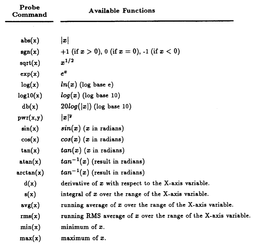
In this text we use the Probe facility available in PSpice. Probe is designed to function like a software version of an oscilloscope. It enables us to use an interactive graphic process to look at results. In addition, Probe has many built-in computational capabilities that allow an interactive investigation of circuit behavior after a completed PSpice simulation. For example, Probe can compute and graphically display the instantaneous power dissipated by a transistor by multiplying its collector current as a function of time by the corresponding collector-emitter voltage.
Table 1.6 lists the most important of the powerful mathematical commands available in Probe, including such functions as integration and differentiation. The variable x used in the argument of each function represents any output variable recognized by Spice, and also network variables generated by PSpice. Table 1.7 lists the variables in PSpice and recognized by Probe.
|
Table 1.6: Probe mathematical functions.
|
Table 1.7: Variables generated by PSpice and recognized by Probe.
|
In order to use Probe, the input file must contain a .Probe statement which causes PSpice to create the necessary data file for Probe's later use. The data file will contain all the network variables associated with the simulation, e.g., the results of DC sweep, AC frequency response and transient response.
Hard copies of any graphical result easily can be created by Probe for future reference. In fact, we use these plots to illustrate the results of most of the simulations in this text.
|
Fig. 1.8: Screen display seen by user of the Probe facility of PSpice. Two cursors are superimposed on the waveform in order to read values directly off the waveform.
|
Fig. 1.9: Screen display seen by user of the Probe facility of PSpice. Two waveforms are present on the same graph with separate cursors placed on each.
|
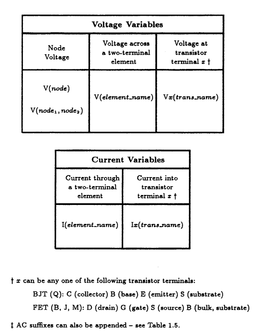
Add a .Probe statement to the Spice deck above and then re-run it. On completion, the results of the PSpice simulation are stored in a special file. Invoking Probe enables us to view the simulation results directly on the monitor screen. Fig. 1.8 displays the actual view of the computer screen we saw when we used Probe to plot the voltage waveform at node 3 of the circuit in Fig. 1.3. In the lower right corner of the screen are the x and y axis values that correspond to the positions of the two cursors on the voltage waveform. The first cursor, C1, is on the second negative peak of the waveform, corresponding to a time of 31.734 ms and a voltage of --69.079 V. The second cursor, C2, is on the second positive peak of the waveform corresponding to a time of 22.734 ms and a voltage of 69.961 V. Below the co-ordinates is the distance between the two cursors. From this difference, we see, for instance, that the peak-to-peak amplitude of this waveform is 139.040 V.
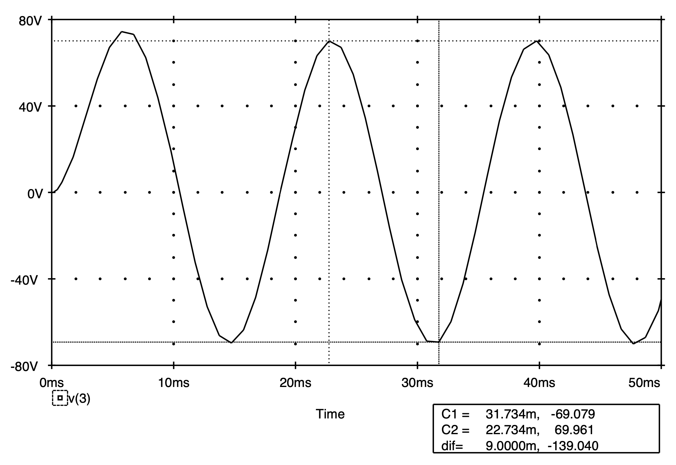
Two or more traces can be added to the same graph, as shown in Fig. 1.9, and the two cursors can be used to access information on either graph. See the PSpice Users' Manual for more details on other variants of these graphical features.
1.4 Examples
The first example involves calculating the DC node voltages of a linear network, the second explores the transient behavior of a three-stage linear amplifier subject to a sine-wave input, the third illustrates how circuit initial conditions are established during a transient analysis, and the last example computes the frequency behavior of a linear amplifier.
1.4.1 Example 1: DC Node Voltages Of A Linear Network
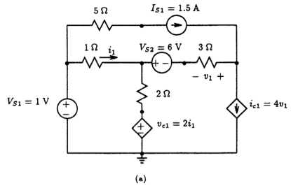
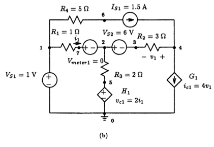
Our first circuit example is shown in Fig. 1.10(a) which displays a rather complicated network of resistors and sources. Sources VS1, VS2, and IS1, are independent DC sources whose values are given on the circuit schematic. The remaining two sources, vc1 and ic1, are dependent sources where vc1 is a current-controlled voltage source (CCVS) and ic1 is a voltage-controlled current source (VCCS). In the case of vc1, the voltage generated by this source is proportional to the current that flows through the 1 W resistor, designated by i1. On the other hand, the current generated by ic1 is proportional to the voltage appearing across the 3 ohm resistor.
The first step in preparing the circuit schematic of Fig. 1.10(a) for a Spice simulation is to identify each element of the circuit by assigning it a unique name, and then, label each node of the circuit with some non-negative integer. It is also necessary to label the ground node of the circuit as node 0. The results of this labeling process are shown in the circuit diagram displayed in Fig. 10.1(b). Further, due to the presence of the CCVS, a zero-valued voltage source must be placed in series with the 1 ohm resistor (R1) in order to sense the current through it. Thus, we have added a zero-valued voltage source Vmeter1 in series with R1. Recall form Table 1.7 that this is a necessary requirement for describing current-controlled sources to Spice.
|
Fig. 1.10: (a) Resistive network with dependent sources. (b) Each node is assigned a non-negative integer number and each element is assigned a unique name. Also, a zero-valued voltage source is placed in series with R1 to monitor the current denoted by i1.
|
Resistive Network With Dependent Sources
** Circuit Description ** * signal sources Vs1 1 0 dc 1V Vs2 2 3 dc 6V Is1 6 4 dc 1.5A * resistors R1 1 7 1ohm R2 3 4 3ohm R3 2 5 2ohm R4 1 6 5ohm * CCVS with ammeter H1 5 0 Vmeter1 2 Vmeter1 7 2 0 *VCCS G1 4 0 4 3 4
** Analysis Requests ** * compute DC solution .OP
** Output Requests ** * by default the ".OP" command prints all node voltages .end
Fig.1.11: Spice input deck for the circuit shown in Fig. 1.10(b).
|
|
**** SMALL SIGNAL BIAS SOLUTION TEMPERATURE = 27.000 DEG C ******************************************************************************
NODE VOLTAGE NODE VOLTAGE NODE VOLTAGE NODE VOLTAGE
( 1) 1.0000 ( 2) .8462 ( 3) -5.1538 ( 4) -4.8077
( 5) .3077 ( 6) -6.5000 ( 7) .8462
VOLTAGE SOURCE CURRENTS NAME CURRENT
Vs1 -1.654E+00 Vs2 -1.154E-01 Vmeter1 1.538E-01
TOTAL POWER DISSIPATION 2.35E+00 WATTS
**** OPERATING POINT INFORMATION TEMPERATURE = 27.000 DEG C ******************************************************************************
**** VOLTAGE-CONTROLLED CURRENT SOURCES
NAME G1 I-SOURCE 1.385E+00
**** CURRENT-CONTROLLED VOLTAGE SOURCES
NAME H1 V-SOURCE 3.077E-01 I-SOURCE 2.692E-01
|
Fig. 1.12: DC node voltages of the circuit shown in Fig. 1.10(b). Also shown are the voltages and currents associated with the independent and dependent sources.
Our next step is to describe each element of the network to Spice using the element statements described in the previous sections. The results of this are listed in the Spice input deck shown in Fig. 1.11. The first line of the Spice input deck is the title of this particular example. In this case, ``Resistive Network With Dependent Sources.'' This is then followed by a series of lines describing the circuit to Spice beginning with the comment statement: ** Circuit Description **. Notice that each circuit element description in the Spice input deck corresponds directly with an element of the circuit shown in Fig. 1.10(b). Following this circuit description, we list the analysis command: .OP. This tells Spice to compute the DC node voltages of the circuit. Normally, we would then follow this command, and any other analysis request command, by a series of output requests; however, by default, the .OP command prints all the node voltages into the Spice output file. The final statement is an ``.end'' statement, signifying an end to the Spice input file.
Submitting this input file to Spice for execution, would on completion, result, in part, in the Spice output file shown in Fig. 1.12. The only part not shown is a description of the input circuit which was already given in Fig. 1.11. The results that are shown consist of two parts: a small-signal bias solution and operating point information. The small-signal bias solution refers specifically to the voltages on each node of the circuit relative to node 0 and the current flowing through each independent voltage source. Notice that the current supplied by VS1 and VS2 is negative. Thus, according to the Spice convention (positive current flows from the positive terminal of the voltage source to its negative terminal) both currents are actually flowing away from the positive terminal of each source. Also calculated, and included in the output file, is the total power dissipated by the circuit. The second part of output file refers to the DC operating point information of the dependent sources. Specifically, the controlled signal (not the controlling signal) of each dependent source is listed in the output file. In the case of dependent voltage sources, both the controlled voltage and the current it supplies to the circuit are given. The current that controls this source is the current that flows through Vmeter1 (1.538E-01) seen listed in the ``SMALL SIGNAL BIAS SOLUTION’’.
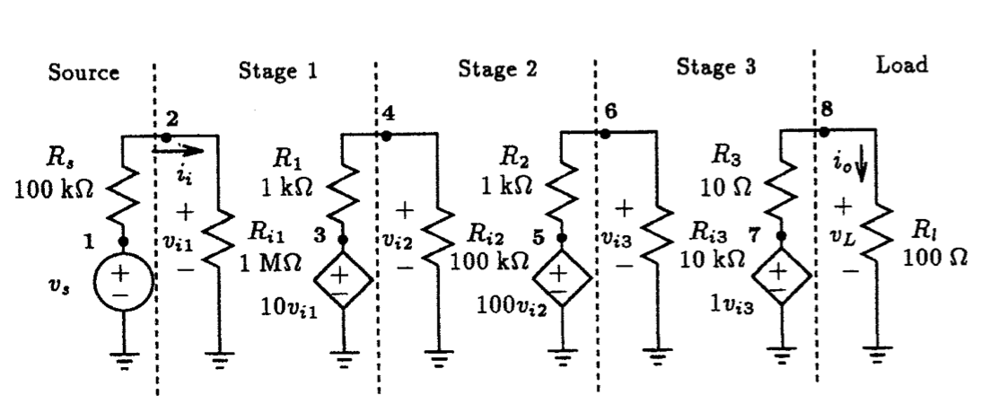
1.4.2 Example 2: Transient Response of A 3-Stage Linear Amplifier
Our next example is shown in Fig. 1.13 which consists of a three-stage linear amplifier fed by a signal source having a source resistance of 100 kW. This example was first encountered in section 1.5 of the text by Sedra and Smith where they computed by hand the overall voltage gain, Av = vL / vs, to be 743.6 V/V, the current gain, Ai=io / ii, to be 8.18 x 10⁶ A/A, and the power gain, Ap=Av x Ai, to be 98.3 dB. Here we shall compute the same gains by using the transient analysis capability of Spice and the graphical post-processing features of Probe and compare the results with those found by hand.
We begin our analysis by creating the Spice circuit description shown in Fig. 1.14 for the circuit of Fig. 1.13. All nodes have been pre-labeled except for the ground node which is assumed to be node 0. The input generator is a 1-volt time-varying sinusoidal voltage source of 1 Hz frequency with zero voltage offset. Using the .TRAN statement we are instructing PSpice to calculate the time response of the circuit from t=0 to t=5 s in 10 ms time steps. Instead of specifying a specific output request, we will simply utilize Probe, the graphical post-processor facility of PSpice, to compute the various signal gains. This requires that we enter the .Probe command into the Spice input file as shown in Fig. 1.14.
|
Fig. 1.13: A three stage amplifier with input signal and load.
|
Transient Response Of A 3-Stage Linear Amplifier
** Circuit Description ** * signal source Vs 1 0 sin (0V 1V 1Hz) Rs 1 2 100k * stage 1 Ri1 2 0 1Meg E1 3 0 2 0 10 R1 3 4 1k * stage 2 Ri2 4 0 100k E2 5 0 4 0 100 R2 5 6 1k * stage 3 Ri3 6 0 10k E3 7 0 6 0 1 R3 7 8 10 * output load Rl 8 0 100
** Analysis Requests ** * compute transient response from t=0 to 5s in time steps of * 10ms with an internal time-step no greater than 10ms. .TRAN 10ms 5s 0s 10ms
** Output Requests ** * graphical post-processor .PROBE .end
Fig. 1.14: Spice input deck for circuit shown in Fig. 1.13.
|
On completion of Spice, we use Probe to view the results. In Fig. 1.15(a) we plot both the input voltage (v(1)) and output voltage (v(8)) as a function of time. The range of the y-axis is set equal to the peak-to-peak value of the signal shown. Because the two signals are in phase, the voltage gain V(8)/V(1) is simply the ratio of the peak values, which, in this case, is 743.8 V/V.
On completion of Spice, the results of this analysis can be viewed using the Probe facility of PSpice. In Fig. 1.15(a) we plot both the input voltage (v(1)) and output voltage (v(8)) as a function of time. The range of the y-axis was set equal to the peak-to-peak value of the signal that is shown. Because the two-signals are in-phase, the voltage gain V(8)/V(1) is simply the ratio of the peak values, which, in this case, turns out to be 743.8 V/V.
Similarly, the waveforms of the input current (ii=i(Ri1)) and the load current (io=i(Rl)) are shown in Fig. 1.15(b). The resulting current gain provided by this network is then calculated to be 8.18 MA/A.
As a final calculation, Probe was used to compute and display the instantaneous power delivered to the amplifier stage (v(2) x i(Ri1)) and to its load (v(8)xi(Rl)). These waveforms are shown in Fig. 1.15(c). The power gain is then found to be 6.69 GW/W or 98.3 dB.
|
(a) |
(b) |
(c) |
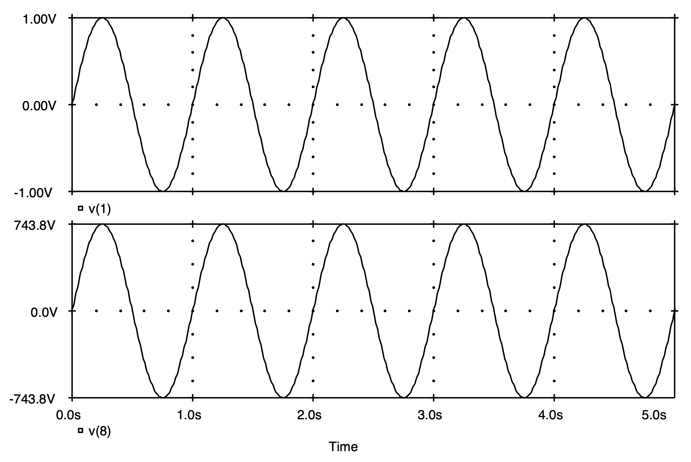
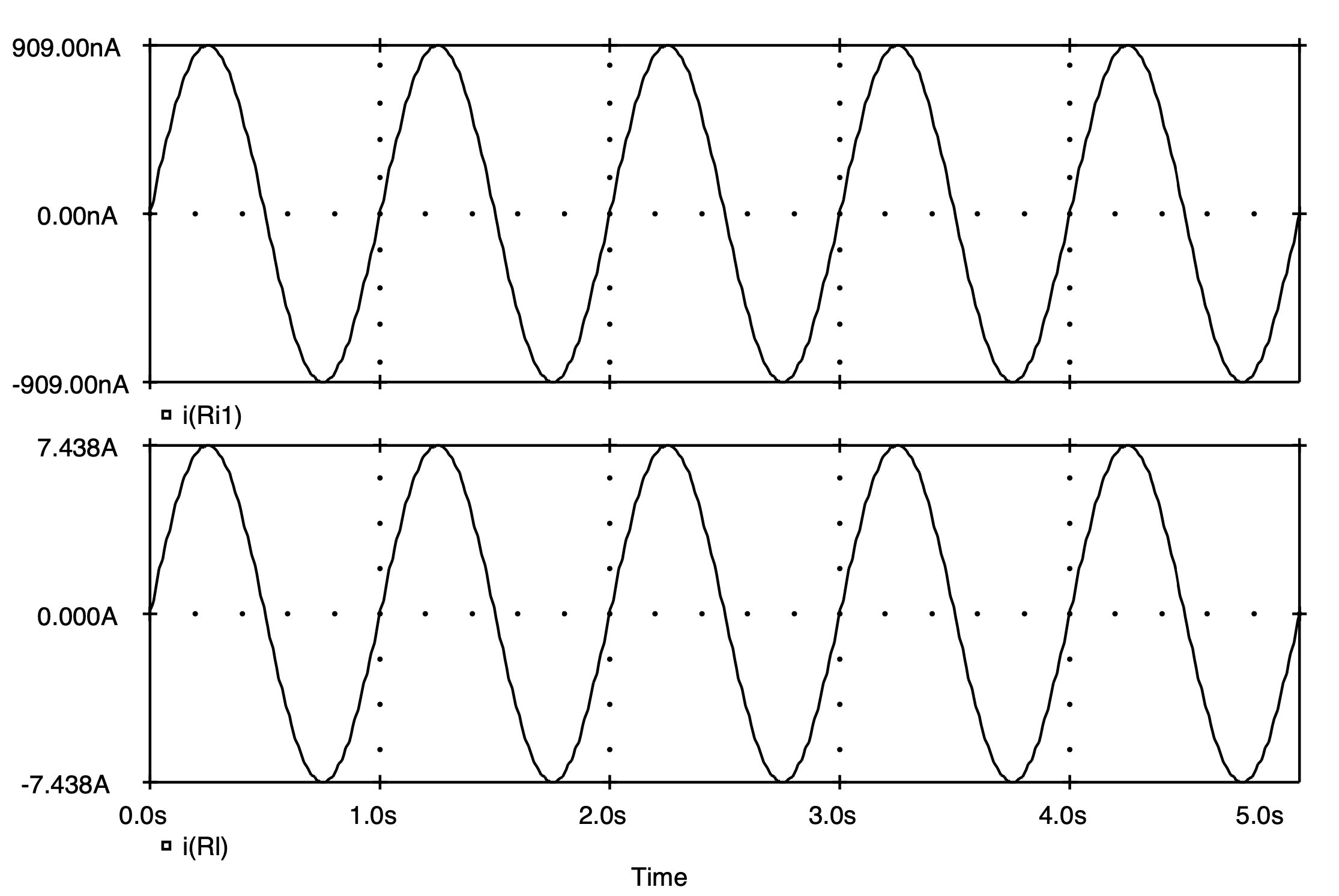
Fig. 1.15: Various transient results for the circuit of Fig. 1.13: (a) input and output voltage signals; (b) input and output current signals; (c) power delivered to amplifier and load.
|
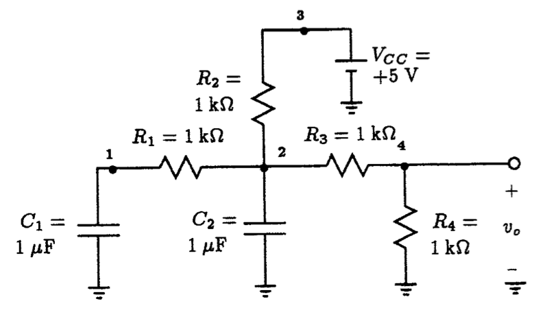
Fig. 1.16: An RC network for investigating the different ways in which Spice sets the initial conditions prior to the start of a transient analysis.
|
Investigating Initial Conditions Established By Spice
** Circuit Description ** Vcc 3 0 DC +5V R1 1 2 1k R2 3 2 1k R3 2 4 1k R4 4 0 1k C1 1 0 1uF C2 2 0 1uF
** Analysis Requests ** .Tran 500us 10ms 0ms 500us
** Output Requests ** .PLOT TRAN V(1) V(2) V(4) .probe .end
Fig. 1.17: Spice input deck for circuit shown in Fig. 1.16. No explicit initial conditions are indicated.
|
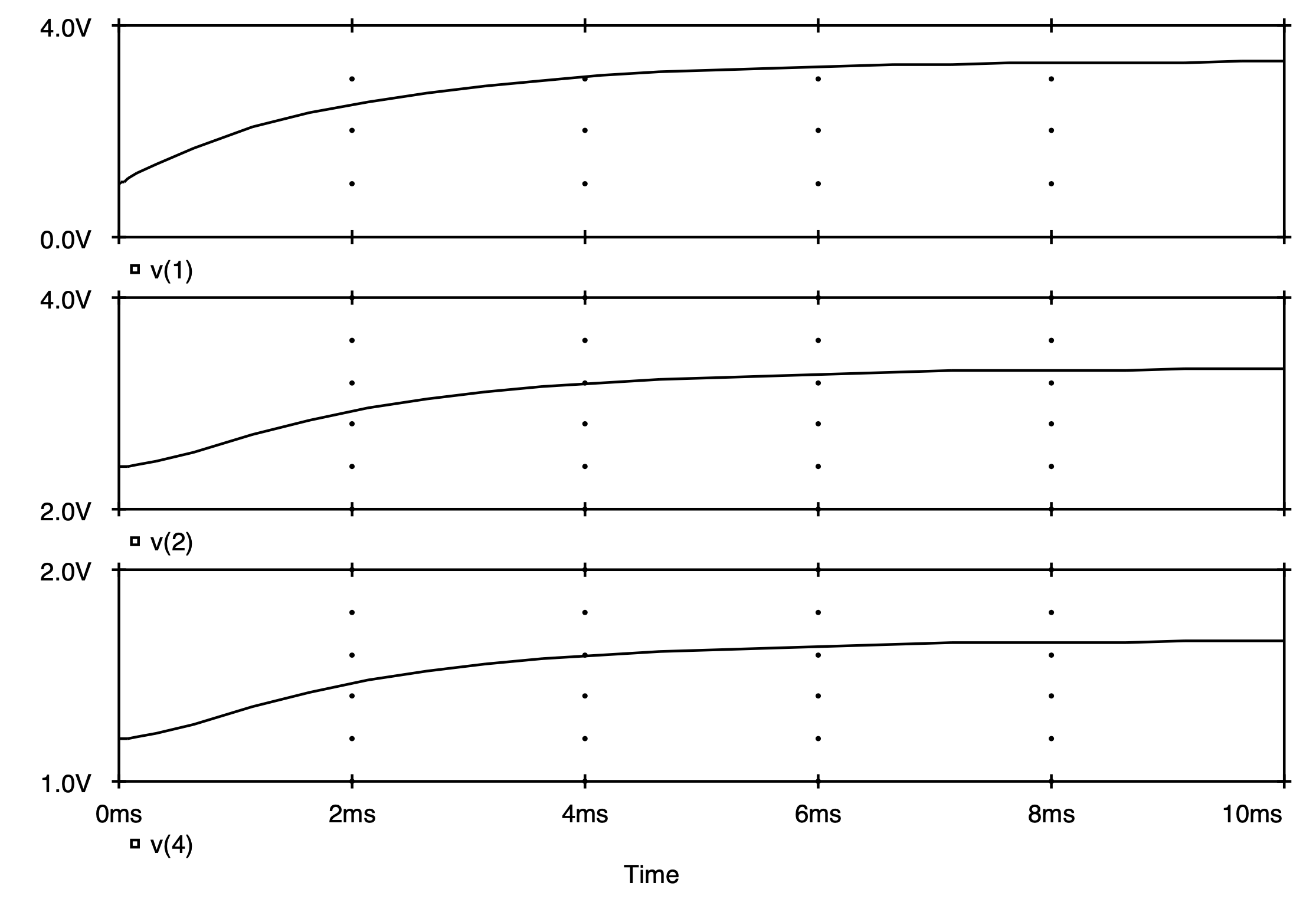
1.3.3 Example 3: Setting Circuit Initial Conditions During A Transient Analysis
There are three ways to set the initial conditions of a circuit at the start of a transient analysis. We demonstrate these on the simple RC circuit in Fig. 1.16.
In the first case, let us begin our transient analysis with the DC operating point of the circuit establishing the initial conditions for the circuit. The Spice input file for this circuit is shown in Fig. 1.17. The transient analysis request seen there simply commands Spice to compute the behavior of the RC circuit over a 10 ms interval using a 500 ms step interval. For the purpose of comparison, we shall request that Spice plot the voltages across each capacitor as well as the voltage that appears at the output terminals. In this way, we can observe the initial conditions established by Spice at the start of the transient analysis and the effect that they have on the output.
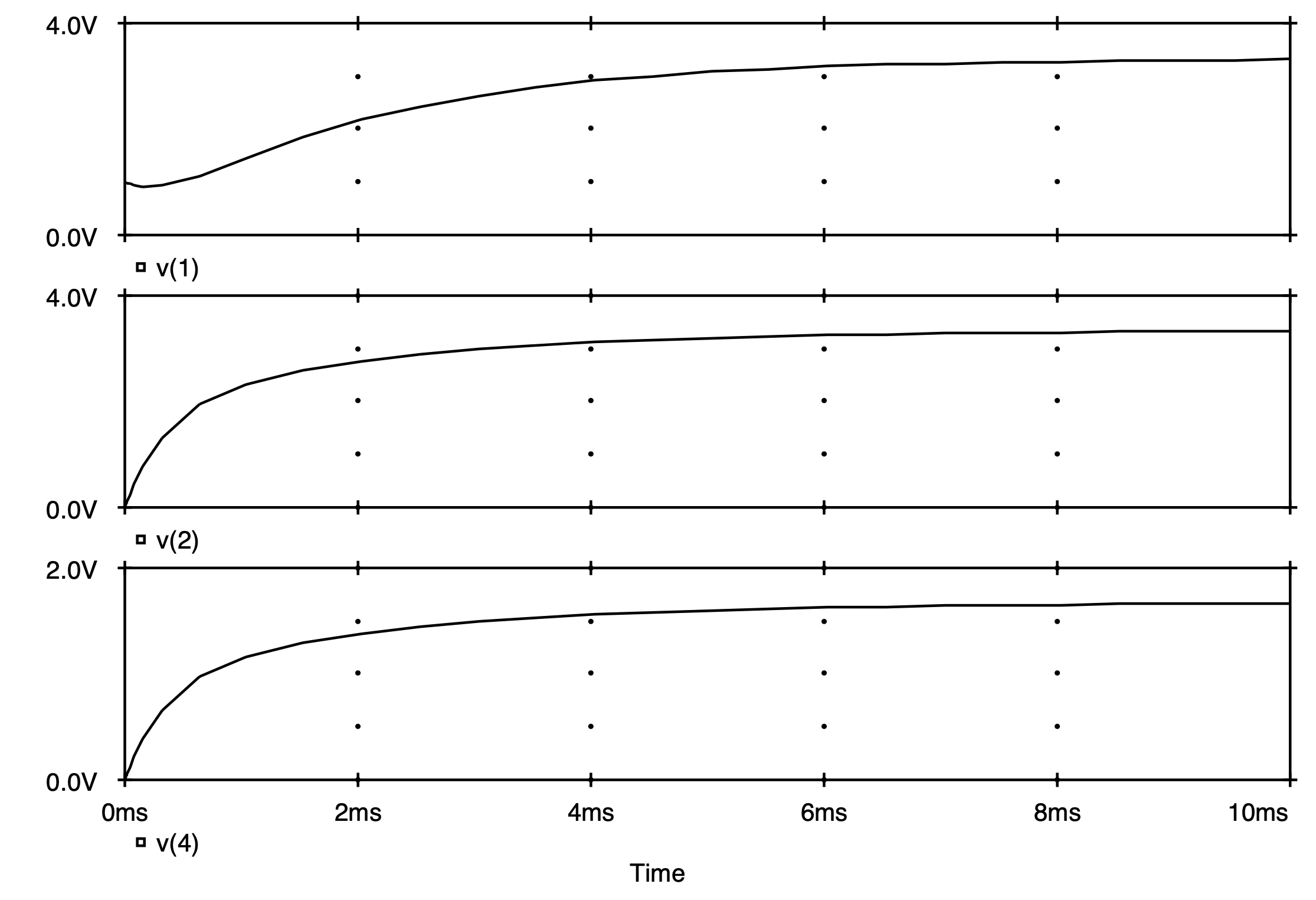
On completion of Spice, the results of the analysis are shown plotted in Fig. 1.18. The top graph displays the voltage appearing across capacitor C1, the middle graph displays the voltage appearing across capacitor C2, and the bottom graph displays the voltage appearing at the output. As is clearly evident in all three cases, no change in the output voltage is taking place. This suggests that the initial conditions found by Spice were also the final time values. To illustrate that these initial conditions correspond to the DC operating point solution, we list below the results of an .OP analysis:
**** SMALL SIGNAL BIAS SOLUTION TEMPERATURE = 27.000 DEG C
******************************************************************************
NODE VOLTAGE NODE VOLTAGE NODE VOLTAGE NODE VOLTAGE
( 1) 3.3333 ( 2) 3.3333 ( 3) 5.0000 ( 4) 1.6667
Let us consider setting the initial voltage across capacitor C1 at +1 V and observe the effect that it has on the circuit operation. To do this, we simply modify the element statement for C1 according to
C1 1 0 1uF IC=+1V
and specify that Spice use this initial condition by attaching on the end of the .TRAN statement the flag ``UIC'' according to
.TRAN 500us 10ms 0ms 500us UIC.
The results of this analysis are shown in Fig. 1.19. Unlike the previous case, the voltages in the circuit are now changing with time. At time t=0, we see that the voltage across capacitor C1 is +1 V, as expected. The voltage across C2 at this time is 0 V by default (since it was not specified in the Spice deck), and as a result, the output voltage is initially zero. As time progresses, we see that these three voltages converge to values identical to those found in the previous case (i.e. 3.33 V, 3.33 V and 1.667 V, respectively).
Another way of setting the initial conditions is with the .IC command line. This method is essentially a combination of the two previous methods. The specific node voltages can be explicitly set, and the remaining nodes will take on values that result from the DC operating point analysis (with the initial value of appropriate nodes taken into account) instead of defaulting to zero.
For example, let us set the voltage at node 1 by using the following .IC command line:
.IC V(1)=+1V
We change the element statement for C1 back to its original form,
C1 1 0 1uF
and remove the UIC flag on the .TRAN statement:
.TRAN 500us 10ms 0ms 500us.
The results of this analysis are shown in Fig. 1.20. Here we see that at time t=0 the voltage at node 1 begins at +1 V as specified. In contrast to the previous case, the voltage at the second node does not begin at 0 V but instead begins with a value of 2.4 V. Likewise, the output voltage is no longer zero but instead begins at a voltage level of 1.20 V. The final values settle to the same values found previously in the other two cases.
|
Fig. 1.18: Voltage waveforms associated with the RC circuit shown in Fig. 1.16. No initial conditions were explicitly given, instead the DC operating point solution is used as the circuit initial conditions. The top graph displays the voltage appearing across capacitor C1, the middle graph displays the voltage appearing across capacitor C2, and the bottom graph displays the voltage appearing at the output.
|
Fig. 1.19: Voltage waveforms associated with the RC circuit shown in Fig. 1.16 when the voltage across capacitor C1 is initially set to +1 V using IC=+1V on the element statement of this capacitor.
|
Fig. 1.20: Voltage waveforms associated with the RC circuit shown in Fig. 1.16 when the voltage at node 1 is initially set to +1 V using an. IC command.
|
1.4.4 Example 4: Frequency Response Of A Linear Amplifier
The final example of this chapter demonstrates how Spice is used to compute the frequency response of a linear amplifier. Fig. 1.21 shows the small-signal equivalent circuit of a one-stage amplifier, and Fig. 1.22 is the corresponding Spice input file used to describe it. The input to the circuit is a 1 V AC voltage source whose frequency will be varied between 1 Hz and 100 MHz logarithmically with 5 points-per-decade, as is indicated by the .AC analysis command. By selecting a 1 V input level, the output voltage level will also correspond to the voltage transfer function Vo/Vs since Vs=1.
The frequency response behavior of this amplifier was calculated by Spice and the magnitude and phase of the output voltage Vo was plotted using Probe. The plot seen on the screen of the computer monitor is shown in Fig. 1.23. It consists of two graphs: the top graph indicates the magnitude response and the bottom graph indicates the phase response of the amplifier. As a rough estimate of the 3-dB bandwidth of this amplifier, we see from this graph that it ranges somewhere around 100 kHz. A better estimate of the 3-dB bandwidth is obtained using the cursor facility of Probe and found to be 158.5 kHz.
|
Fig. 1.21: A frequency-dependent voltage amplifier with signal input and load.
|
Frequency Response Behavior Of A Voltage Amplifier
** Circuit Description ** * signal source Vs 1 0 AC 1V Rs 1 2 20k * frequency-dependent amplifier Ri 2 0 100k Ci 2 0 60p Eamp 3 0 2 0 144 Ro 3 4 200 * load Rl 4 0 1k
** Analysis Requests ** * compute AC frequency response from 1 Hz to 100 MHz * using 5 frequency steps per decade. .AC DEC 5 1 100Meg
** Output Requests ** * print the magnitude and phase of the output voltage * as a function of frequency .PRINT AC Vm(4) Vp(4) .PROBE .end
Fig. 1.22: Spice input deck for circuit shown in Fig. 1.21.
|
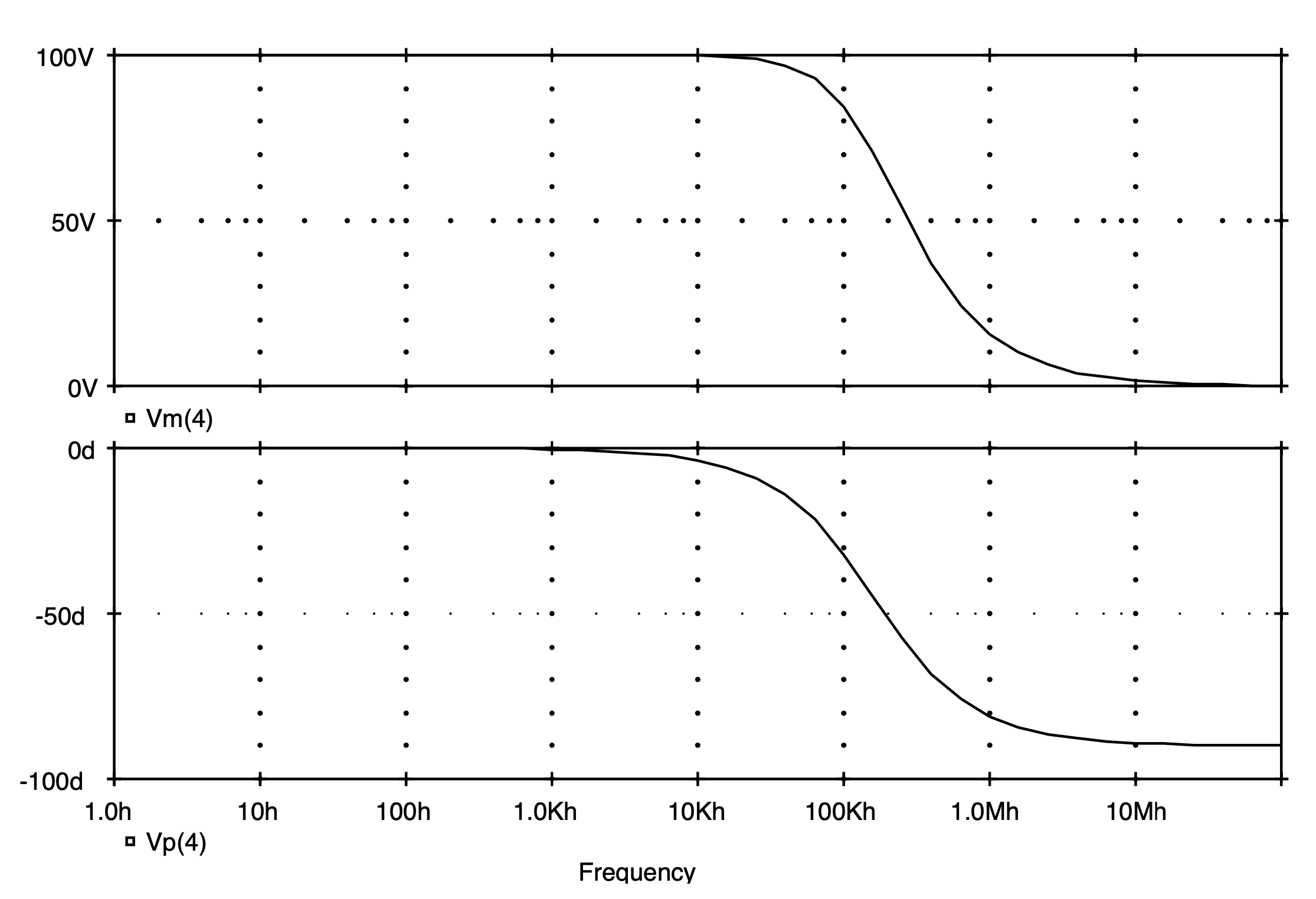
Fig. 1.23: The magnitude and phase response behavior of the amplifier circuit shown in Fig. 1.21.
1.4 Spice Tips
· Spice is an acronym for Simulation Program with Integrated Circuit Emphasis. It was originally developed for large main-frame computers.
· PSpice is a PC version of Spice and a student version is distributed freely by MicroSim Corporation.
· Circuits are designed by people not computers; Spice can only verify operations of human-designed circuits.
· A Spice input file consists of three main parts: circuit description, analysis requests and output requests.
· The first line in a Spice input file must be a title statement and the last line must be an. end statement.
· A circuit is described to Spice by a sequence of element statements describing how each element is connected to the rest of the circuit and specifying its value.
· Each element type has a unique first-letter representation, e.g., R for resistor, C for capacitor.
· Spice performs three main analyses: nonlinear DC analysis, transient analysis and small-signal AC analysis.
· Spice can perform other analysis as special cases of the three main analysis types. One example is the DC Sweep command used to compute DC transfer characteristics.
· The results of circuit simulation are placed in an output file in either tabular or graphical form.
· PSpice is equipped with a post-processor called Probe which allows for interactive graphical display of simulation results.
· Probe can perform many powerful mathematical functions such as differentiation and integration on any network variable created during circuit simulation.
1.5 Bibliography
1. A. Vladimirescu, K. Zhang, A. R. Newton, D. O. Pederson, and A. Sangiovanni-Vincentelli, ``SPICE Version 2G6 User's Guide,'' Dept. of Electrical Engineering and Computer Sciences, University of California, Berkeley, CA, 1981.
2. Staff, PSpice Users' Manual, MicroSim Corporation, Irvine, California, Jan. 1991.
1.7 Problems
1.1. For each of the circuits shown in Fig. P1.1 compute the corresponding node voltages using Spice.
1.2. For each of the circuits shown in Fig. P1.2 compute the corresponding node voltages and branch currents indicated using Spice.
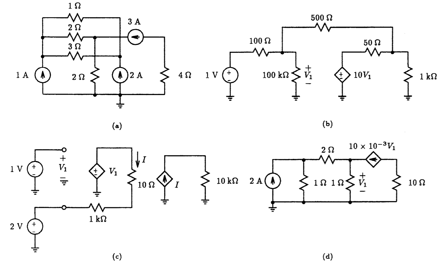
Fig. P1.1
1.3. Using the simple circuit arrangement shown in Fig. P1.3, generate a voltage waveform across the 1-ohm resistor having the following described form:
(i) 10 sin ( 2p x 60 t )
(ii) 1 + 0.5 sin ( 2p x 1000t )
(iii) 1 + 1 e-0.005t sin ( 2p x 100 t )
(iv) ![]()
Verify your results using Spice by plotting the voltage waveform that appears across the 1-ohm resistor for at least 6 cycles of its waveform. Use a time step that samples at least 20 points on one cycle of the waveform.
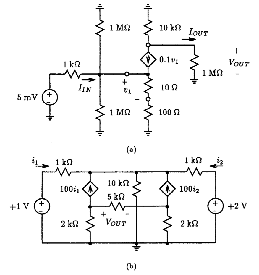
Fig. P1.2
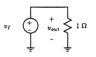
Fig. P1.3
1.4. Using the simple circuit arrangement shown in Fig. P1.3, generate a voltage waveform across the 1-ohm resistor having the following described form:
(i) 10 V peak-to-peak symmetrical square-wave at a frequency of 1 kHz. Let the rise and fall times be 0.1% of the total period of the waveform.
(ii) 8 V peak-to-peak asymmetrical square-wave at a frequency of 100 kHz having a DC offset of 2 V. Assign the rise and fall times of this waveform to be 0.1% of the total period of this waveform.
(iii) 10 V peak-to-peak asymmetrical square-wave at a frequency of 5 kHz having a DC offset of 2 V. Let the rise and fall times be 0.1% of the total period of the waveform.
Verify your results using Spice by plotting the voltage waveform that appears across the 1 W resistor for at least 6 cycles of its waveform. Use a time step that samples at least 20 points on one cycle of the waveform.
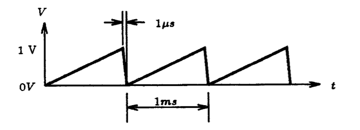
Fig.P1.6
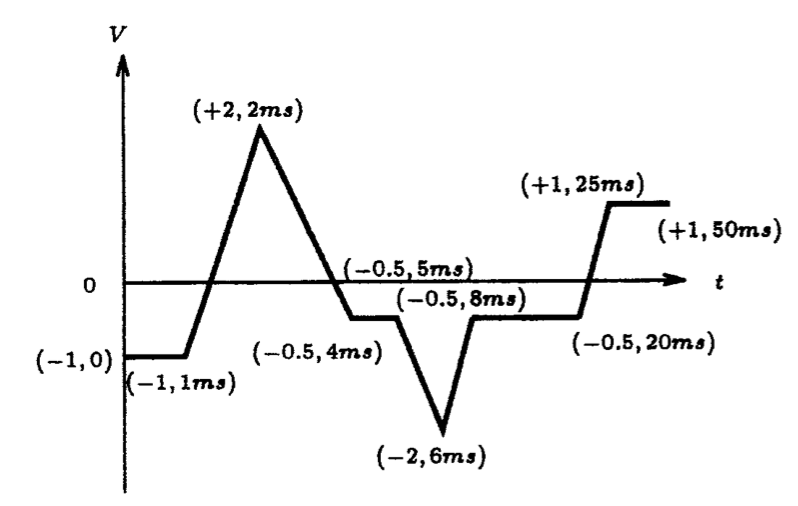
Fig. P1.7
1.5. Replace the voltage source seen in Fig. P1.3 by a current source. Generate a current into the 1 W resistor using the PULSE source statement of Spice such that it has a triangular shape with an amplitude of 2 mA and a period of 2 ms. The average value of the waveform is zero. Plot this current for at least 6 cycles of its waveform using 10 points per period. Hint: Spice will not accept a pulse width of zero, so use a value that is at most 0.1% of the pulse period.
1.6. Using the PULSE source statement of Spice, together with the circuit setup shown in Fig. P1.3, generate the saw-tooth voltage waveform shown in Fig. P1.6. Verify your results by plotting the voltage across the 1 W resistor for at least 6 cycles of its waveform.
1.7. Using the PWL source statement of Spice, together with the circuit setup shown in Fig. P1.3, generate the voltage waveform shown in Fig. P1.7. Verify your results by plotting the voltage across the 1 W resistor for the full duration of this waveform. What voltage appears across the 1 W resistor if the simulation time extends beyond 50 ms?
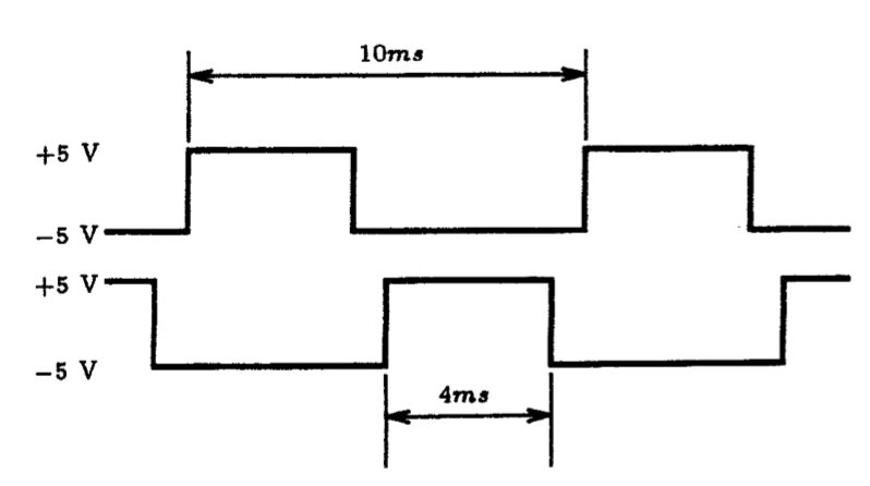
Fig. P1.8
1.8. Using two voltage sources with appropriate loads, generate two signals that are non-overlapping complementary square-waves, such as those shown in Fig. P1.8. Verify your results by plotting the voltage across each load resistor for at least 10 cycles of each waveform.
1.9. Using the simple circuit arrangement shown in Fig. P1.3, generate a 0 to 1 V step signal across the 1 W resistor having a rise-time of no more than 1 us. Verify your results using Spice by plotting the voltage waveform that appears across the 1-ohm resistor for at least 1 ms using a 50 us time step.
1.10. For the first-order RC circuit shown in Fig. P1.10, simulate the behavior of this circuit with Spice subject to a 0 to 1 V step input having a rise time of no more than 10 ns. Plot the voltage waveform that appears across the 1 k-ohm resistor and the 1 uF capacitor. Verify that the voltage across the capacitor changes by 63% of its final value in a time of one time constant.
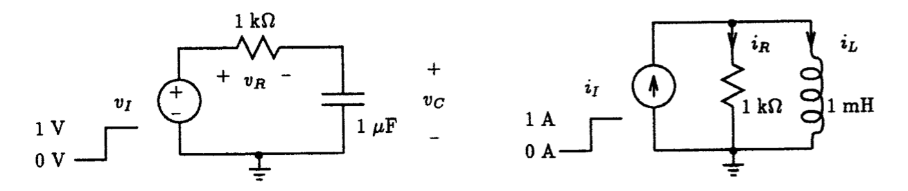
Fig. P1.10 Fig. P1.11
1.11. For the first order RL circuit shown in Fig. P1.11, simulate the behavior of this circuit with Spice subject to a 0 to 1 A step input having a rise time of no more than 10 ns. Plot the current that flows in both the 1 k-ohm resistor and the 1 mH inductor. Verify that the current that flows in the inductor changes by 63% of its initial value in one time constant. Hint: One way of monitoring the current through a resistor or inductor is to connect a zero-valued voltage source in series with that element.
1.12. Repeat Problem P1.10 with the 1 uF capacitor initially charged to 0.5 V.
1.13. Repeat Problem P1.11 with the 1 mH inductor initially conducting a current of 2 A.
1.14. For the first-order RC circuit shown in Fig. P1.10 subject to a 1 V peak sine-wave input signal of 1 kHz frequency, simulate the behavior of this circuit with Spice. Plot the voltage waveform that appears across the 1 uF capacitor for at least 6 cycles of the input signal. Use a time step that acquires at least 20 points per period.
1.15. Repeat Problem P1.14 with a 1 V peak symmetrical square-wave input of 10 kHz frequency. How would you describe the voltage waveform that appears across the capacitor?
1.16. For the first order RL circuit shown in Fig. P1.11 subject to a 1 A peak-to-peak triangular input signal of 1 kHz frequency, simulate the behavior of this circuit with Spice. Plot the current waveform that flows through the 1 k-ohm resistor for at least 6 cycles of the input signal. Use a time step that acquires at least 20 points per period. How would you describe this current waveform?
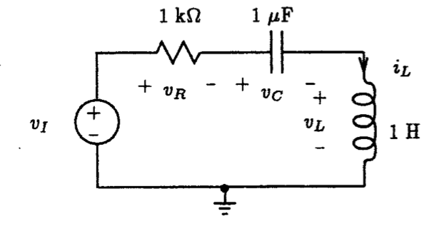
Fig. P1.17
1.17. For the second order RLC circuit shown in Fig. P1.17 subject to a 1 V step input, simulate the transient behavior of the circuit and plot the voltage waveform that appears across each element for about 40 ms. Use a time step of no more than 100 us.
1.18. Repeat Problem 1.17 with value of the resistor decreased by a factor of 10. How do the waveforms compare with that in Problem 1.17.
1.19. Repeat Problem 1.17 with value of the resistor decreased by a factor of 100. How do the waveforms compare with that in Problem 1.17.
1.20. Compute the frequency response behavior of the RC circuit shown in Fig. P1.10 using Spice for a 1 V AC input signal. Plot both the magnitude and phase behavior of the voltage across the resistor and the voltage across the capacitor over a frequency range of 0.1 Hz to 10 MHz. Use 20 points-per-decade in your plot.
1.21. Compute the frequency response behavior of the RL circuit shown in Fig. P1.11 using Spice for a 1 A, AC input signal. Plot both the magnitude and phase behavior of the current through the resistor and inductor over a frequency range of 1 mHz to 1 MHz. Use 10 points-per-decade in your plot.
1.22. Compute the frequency response behavior of the RLC circuit shown in Fig. P1.17 using Spice for a 1 V AC input signal. Plot both the magnitude and phase behavior of the voltage across the resistor, inductor and capacitor over the frequency range of 1 Hz to 1 kHz. Use 10 points-per-octave in your plot.
1.23. Compute the frequency response behavior of the RLC circuit shown in Fig. P1.17 with R having values of 10, 100 and 1 kW. Plot the magnitude and phase response of each case and compare them. Select an appropriate frequency range and number of points that best illustrate your results.