Chapter 13
MOS Digital Circuits
In this chapter the basic operation of several types of simple MOS digital circuits will be investigated with the aid of Spice. Of particular interest are those digital circuits constructed in NMOS, CMOS or GaAs integrated circuit technologies. Our discussion here will mainly involve the static and dynamic analysis of several basic inverter circuits found in these three technologies, but some analyses of a two-input NOR gate and a D-type flip-flop will also be performed.
13.1 NMOS Inverter with Enhancement Load
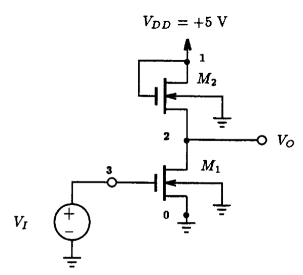
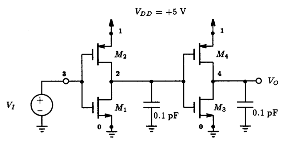
As the first example of this chapter we have on display in Fig.13.1 an NMOS inverter circuit with an enhancement load with the substrate connected to ground. Although, the source-to-body voltage (VSB) of M1 is zero, that of M2 is equal to VO. As a result, the threshold voltage of M2 is no longer equal to the threshold voltage of M1. For straightforward hand analysis, it is common to neglect the transistor body effect and assume that each transistor has the same threshold voltage. However, as we shall see from the following Spice circuit simulations of the inverter circuit shown in Fig.13.1, neglecting the body effect results in substantial error in the large-signal input-output transfer characteristics. This is especially true for input signal levels near ground potential.
|
Fig. 13.1: The enhancement-load inverter with substrate connected to ground. |
An Enhancement-Load Inverter
** Circuit Description ** * dc supplies Vdd 1 0 DC +5V * input digital signal Vi 3 0 DC 0V * MOSFET circuit M1 2 3 0 0 nmos_enhancement_mosfet L=3um W=9um M2 1 1 2 0 nmos_enhancement_mosfet L=9um W=3um * mosfet model statement (by default level 1) .model nmos_enhancement_mosfet nmos (kp=40u Vto=0.7V phi=0.6V gamma=1.1) ** Analysis Requests ** .DC Vi 0V +5V 100mV ** Output Requests ** .Plot DC V(2) .probe .end
Fig. 13.2: The Spice input file for calculating the input-output voltage transfer characteristics of the enhancement-load inverter circuit shown in Fig. 13.1.
|
The Spice input description of the inverter circuit shown in Fig. 13.1 is seen listed in Fig. 13.2. The parameters associated with each transistor of the inverter are assumed as follows: Vto=0.7 V, W1=9 μm, L1=3 μm, W2=3 μm, L2=9 μm, μnCOX= 40 μA/V2,2ff=0.6 V. Each transistor is also assumed to have a body effect coefficient (gamma) equal to 1.1 V1/2.
|
Fig. 13.3: The input-output voltage transfer characteristics of the enhancement-load inverter circuit shown in Fig. 13.1 with and without the body effect present.
|
Fig. 13.4: dVO/dVI as a function of the input voltage level VI with and without the body effect present. These curves are used to determine the minimum inverter input voltage VIH. |

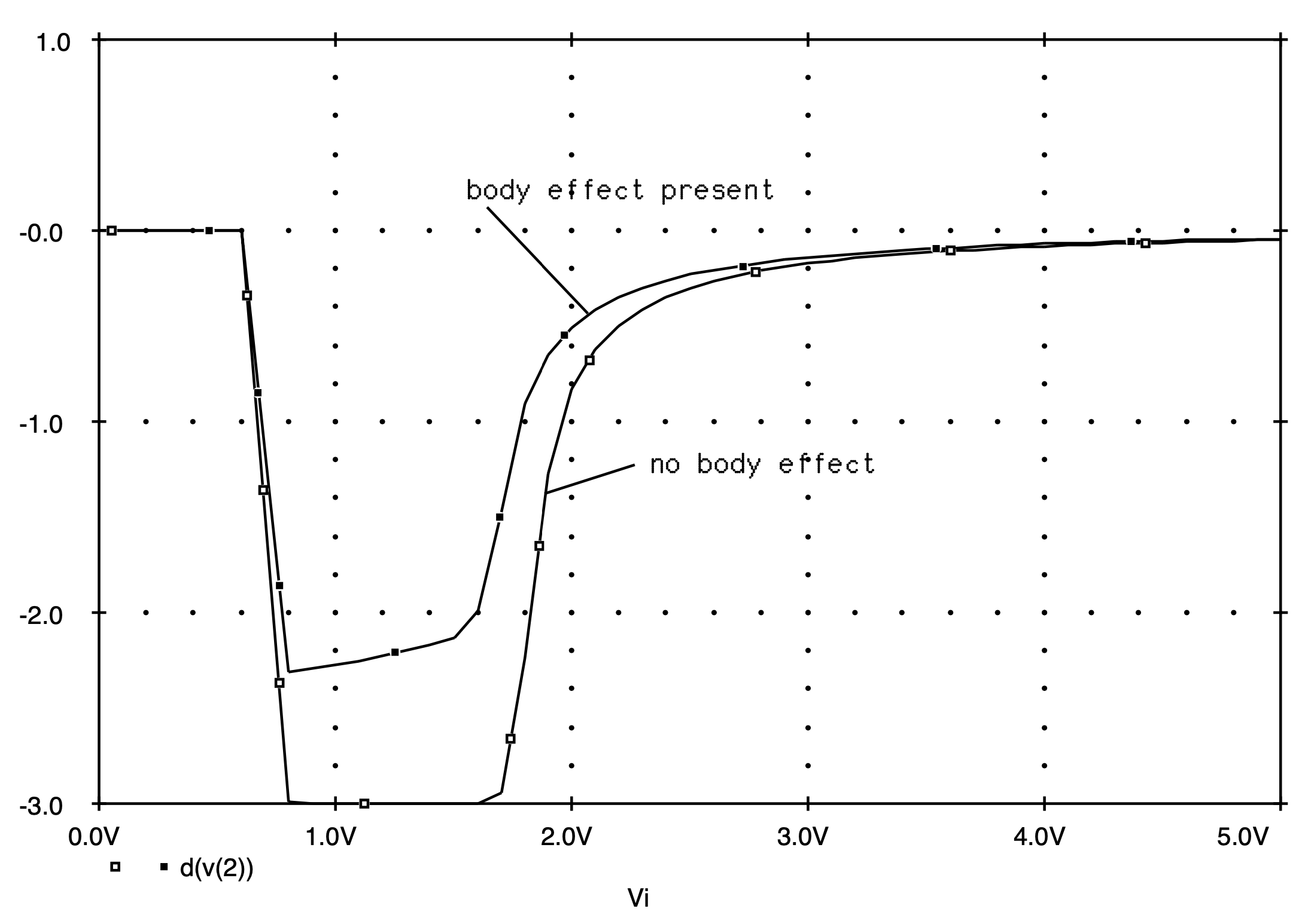
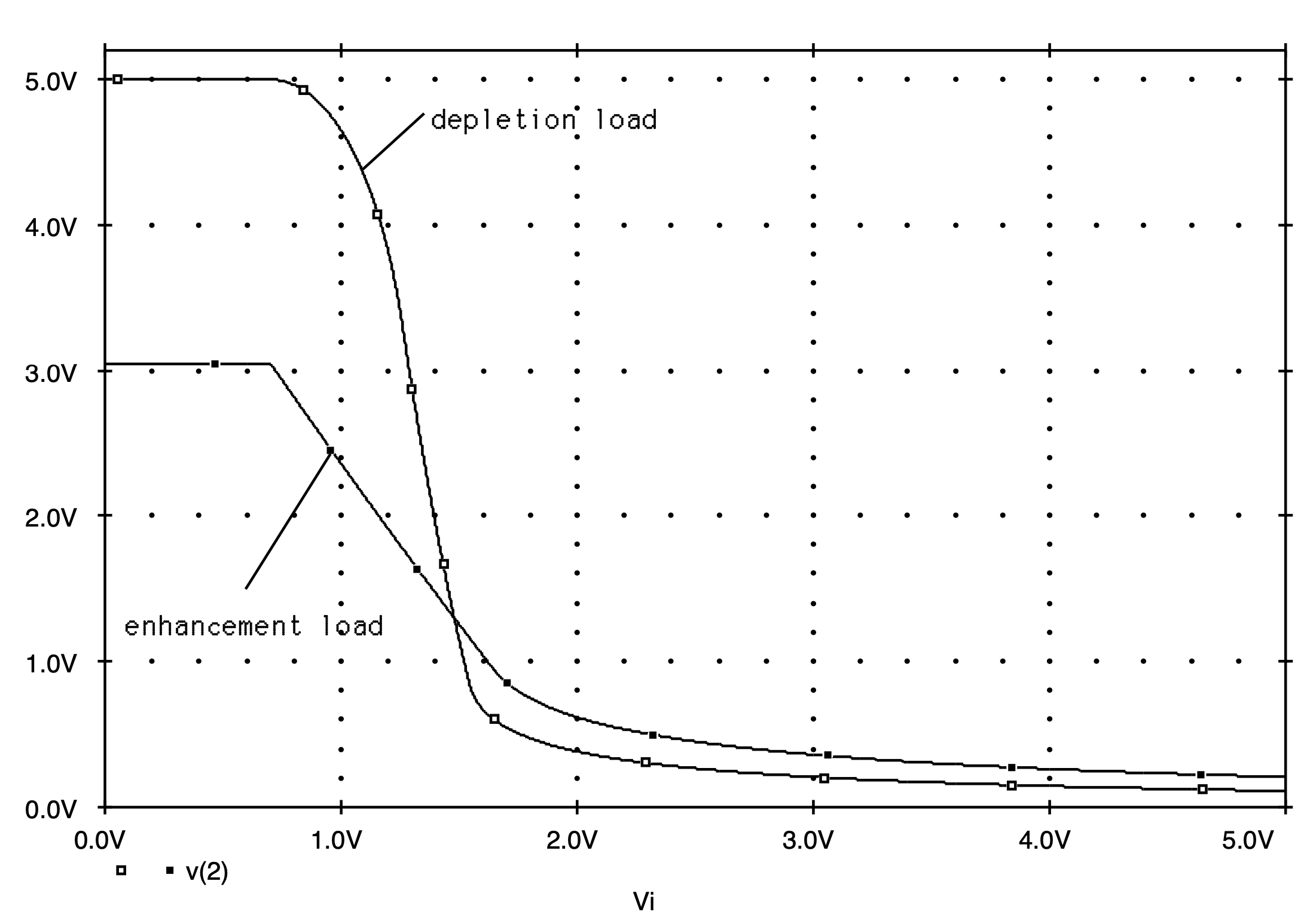
The results of the computer simulation are shown in Fig. 13.3. Superimposed on the same graph are the input-output transfer characteristics of the inverter circuit when the body effect is eliminated (i.e., set gamma=0 on the transistor model statement in Fig. 13.2 and re-run the Spice analysis). Clearly, at low input levels, the two curves differ significantly, whereas, for higher input levels (VI > 2.5 V), the two results agree quite closely.
It is interesting to compare the noise margins of these two situations. From Fig. 13.3, we see directly using Probe from the transfer characteristics accounting for the transistor body effect that VIL=0.7 V, VOL=0.24 V and VOH=3.05 V. To determine VIH, it is necessary to determine the input level where the transfer characteristic has a slope of -1 in the vicinity of a logic low level. This is easy to do with the aid of the derivative procedure command available in PROBE. Taking the derivative of the output voltage (VO) with respect to the input voltage (VI) for the above two cases and plotting it versus the input voltage level, we obtain the graphical results shown in Fig. 13.4. From this we see that the input level in the vicinity of a logic low level corresponding to a slope of -1 is 1.78 V. Thus, VIH=1.78 V. Therefore, the two noise margins for the enhancement-load inverter with body effect included are:
NMH = VOH - VIH = 3.05 - 1.78 = 1.27 V
NML = VIL - VOL = 0.7 - 0.24 = 0.46 V
Carrying out the above procedure for the characteristics of the enhancement-load inverter excluding the body effect we get the following two noise margins:
NMH = VOH - VIH = 4.3 - 1.96 = 2.34 V
NML = VIL - VOL = 0.7 - 0.26 = 0.44 V
On comparison, we see that the body effect has decreased the high noise margin (NMH) from 2.34 V to 1.27 V. The low noise margin (NML) remains relatively unchanged.
To complete our investigation of the static behavior of the enhancement-load inverter circuit, we shall compute its average static power dissipation assuming that the inverter spends equal time in each of its two states. We shall include the body effect in this analysis.
Returning to the Spice deck for the inverter, shown in Fig. 13.2, setting the input to the inverter to logic low, say VI=VIL=0.7 V, will force the inverter into its high state. Replacing the DC sweep command with an .OP analysis command will have Spice compute the power dissipated by the inverter. The results of this analysis indicated that the power dissipated is very low at 5.56 W.
Repeating the above with the input at VI=3.05 V to correspond to an output voltage of VOL for some preceding stage, we find that the static power dissipated by the inverter in its low state has increased substantially to a level of 462 μW. Thus, the average static power dissipated by the inverter with enhancement-load is 231 μW.
|
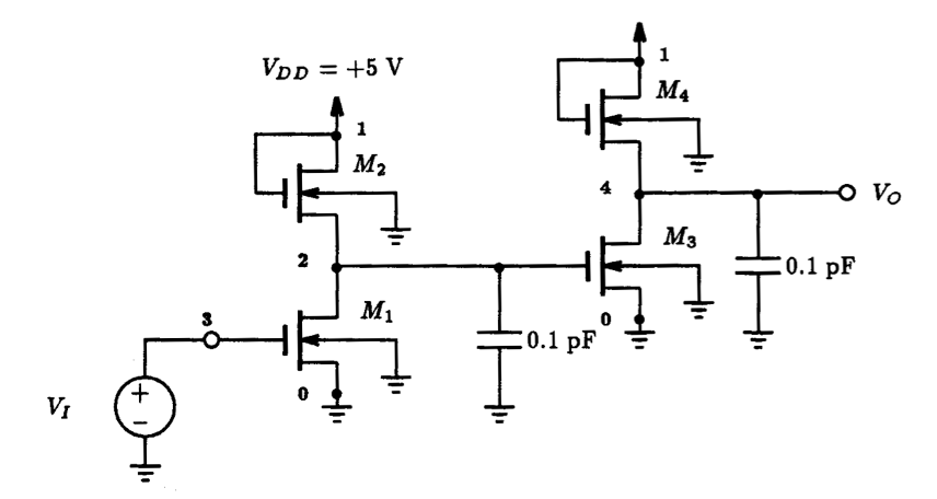
Fig. 13.5: A cascade of two enhancement-load NMOS inverter circuits.
|
A Cascade Of Enhancement-Load Inverters (dynamic effects included)
** Circuit Description ** * dc supplies Vdd 1 0 DC +5V * input digital signal Vi 3 0 PWL (0,0V 10ns,0V 10.1ns,5V 110ns,5V 110.1ns,0V 210ns,0V) * 1st MOSFET inverter circuit M1 2 3 0 0 MN L=3um W=9um M2 1 1 2 0 MN L=9um W=3um Cl1 2 0 0.1pF * 2nd MOSFET inverter circuit M3 4 2 0 0 MN L=3um W=9um M4 1 1 4 0 MN L=9um W=3um Cl2 4 0 0.1pF * BNR 3um transistor model statements (level 3) .MODEL MN nmos (level=3 vto=.7 kp=4.e-05 gamma=1.1 phi=.6 + lambda=.01 rd=40 rs=40 pb=.7 cgso=3.e-10 cgdo=3.e-10 + cgbo=5.e-10 rsh=25 cj=.00044 mj=.5 cjsw=4.e-10 mjsw=.3 + js=1.e-05 tox=5.e-08 nsub=1.7e+16 nss=0 nfs=0 tpg=1 xj=6.e-07 + ld=3.5e-07 uo=775 vmax=100000 theta=.11 eta=.05 kappa=1) ** Analysis Requests ** .TRAN 0.5ns 210ns 0ns 0.5ns ** Output Requests ** .Plot TRAN V(2) V(3) V(4) .probe .end
Fig. 13.6: The Spice input file for computing the transient response for the NMOS inverter cascade shown in Fig. 13.5. |
|
Fig. 13.7: The transient response of a cascade of two enhancement-load NMOS inverter circuits. The top graph displays the input voltage signal and the bottom graph displays the two output voltage signals appearing at each inverter output.
|

Dynamic Operation
We next consider the dynamic operation of the enhancement-load NMOS inverter. To facilitate our investigation, we shall cascade two inverter circuits as shown in Fig. 13.5. The output of each inverter is assumed loaded with a 0.1 pF capacitor to represent the capacitance associated with the interconnect wiring between the two gates. A 0 to 5 V pulse of 100 ns duration is applied to the input of the first inverter circuit. To obtain realistic results, we shall model the NMOS transistors after a commercial 3 μm CMOS process. These model parameters are included in the Spice deck shown in Fig. 13.6. The static parameters remain the same as those seen previously; however, it should be noted that the addition of the other parameters will alter the dc behavior of this circuit somewhat. A transient analysis is requested to be performed over a 200 ns interval using a 0.5 ns time step. The voltage at the output of each inverter will be plotted on completion of Spice.
The transient response of the cascade of inverters as calculated by Spice is presented in Fig. 13.7. The top graph displays the input voltage signal applied to the first inverter and the bottom graph displays the voltage waveform that appears at the output of each inverter circuit. As is evident, the rise time of each inverter is much slower than its fall time. To better estimate the rise and fall times of the inverter, as well as the propagation delay, an expanded view of the high-to-low and low-to-high output transitions of the first inverter is provided in Fig. 13.8.
From Fig. 13.8(a), together with the aid of Probe, we found that the 90% to 10% fall time tTHL is 1.063 ns. This is based on a logic low level VOL of 0.128 V and a logic high value VOH of 3.12 V. In addition, the high-to-low input-to-output delay tPHL was found to be 0.524 ns. Repeating this for the low-to-high output voltage transition shown in Fig. 13.8(b), we find that the 10% to 90% rise time tTLH is 45.9 ns. As well, the low-to-high input-to-output delay tPLH is 7.71 ns. Averaging the above two input-to-output delays, we obtain the propagation time delay tP for the NMOS enhancement-load inverter with a 0.1 pF load to be 4.12 ns.
It is interesting to note that the voltage waveform that appears at the output of the second inverter is somewhat different than that which appeared at the output of the first inverter. This, in turn, gives rise to different transient attributes which include tr, tf and tP. Specifically, we find that the rise time is 38.6 ns and the fall time is 7.95 ns. Also, tPLH=5.81 ns and tPHL=1.28 ns which when combined will give a propagation delay tP of 3.54 ns. The reason the second inverter has different transient attributes from the first inverter stems from to the fact that the signals that appear at the input to each inverter are different. The first inverter has an almost instantaneous voltage change at its input with a rise and fall time of about 0.1 ns, whereas the second inverter see an input voltage signal having an unsymmetrical rise and fall time of 38.6 ns and 7.95 ns, respectively.
|
(a)
|
(b) |
|
Fig. 13.8: An expanded view of the high-to-low and low-to-high output voltage transitions of the first inverter of the circuit shown in Fig. 13.5 when subjected to a step input. |
|


|
Fig. 13.9: The instantaneous power dissipated by the first and second enhancement-load NMOS inverter cascade shown in Fig. 13.5. The top graph displays the power dissipated by the first inverter and the bottom graph displays the power dissipated by the second inverter.
|

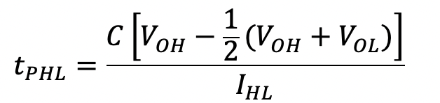
At this stage of our investigation it would be instructive to check the formulae derived by Sedra and Smith, 3rd Edition, in Section 13.2 of their text for estimating the low-to-high and high-to-low transition times tPLH and tPHL, respectively. According to their development,
(13.1)
and
(13.2)
where IHL and ILH represent the average discharge and charge currents. These two currents are obtained from the static characteristics of each device. In terms of the development in Sedra and Smith, with the input VI held high at +5 V (the same logic high level used to compute the transient response of the first inverter shown in Fig. 13.7), together with a simplified set of device parameters obtained from the level 3 NMOS model of the transistor given in the Spice deck of Fig. 13.6, i.e., kp=40 μA/V2, Vt=0.7 V, gamma = 1.1 V1/2 and lambda=0.01 V-1, we find that IHL=861.2 μA and ILH=120.6 μA.
Under the assumption that the effective capacitance seen by the inverter is dominated[1] by the interconnect capacitance of 0.1 pF, we can compute the transition times tPHL and tPLH according to Eqns. (13.1) and (13.2) and obtain:
tPHL=0.174 ns tPLH=1.24 ns.
This can then be averaged to obtain an estimate of the propagation delay time at 0.71 ns. In comparison with the values obtained directly from Spice, tPHL=0.524 ns and tPLH=7.71 ns, we see that the above estimates are off by quite a large amount (for tPLH, a factor of 6).
The reason for such a large discrepancy lies with the assumption that the static parameters of the MOSFET are those seen listed in the level 3 MOSFET model seen in Fig. 13.6. This is, unfortunately, not true. The value of many of the parameters in a level 3 Spice model of a MOSFET have no physical basis; they are simply empirical parameters made to fit the measured device characteristics using a computer optimization algorithm. As such, using a subset of the MOSFET device parameters can, and in this particular case, did, result in significant error. If one makes use of Spice, together with the level 3 MOSFET model, one will find the average discharge and charge currents, IHL and ILH, to be much less than those computed previously at 432 μA and 36 μA, respectively. Substituting these two results into Eqns. (13.1) and (13.2) above, we then obtain:
tPHL=0.347 ns tPLH=4.16 ns.
These two results are much closer to those read directly off the graph of the transient waveform for the first inverter computed by Spice in Fig. 13.8 (i.e., tPHL=0.524 ns and tPLH=7.71 ns). Based on the accuracy of the above two results, we can conclude that Eqns. (13.1) and (13.2) are accurate to only 50% of the actual Spice computed values.
A similar result is obtained when the transition times for the second inverter is computed. By the two formulas given in Eqns. (13.1) and (13.2), together with the average discharge and charge current values of 198 μA and 36 μA, respectively, we find tPHL=0.75 ns and tPLH=4.15 ns. This, in turn, indicates a propagation delay of 2.45 ns. Comparing these results to those directly obtained from Spice (i.e., tPHL=1.28 ns and tPLH=5.81 ns), we once again see that these estimates are within 50% of those found from the transient waveform computed by Spice.
Finally, the instantaneous power dissipated by each inverter circuit of Fig. 13.5 as computed by Spice is shown in Fig. 13.9. The top graph depicts the power dissipated by the first inverter and the bottom graph displays the power dissipated by the second inverter. From the top graph, during the first transition, we see that a sudden power glitch occurs, having a peak power of about 1.46 mW. This occurs as the inverter moves from the logic high to logic low state. After this, the power dissipated by this inverter settles into a steady-state value of 272.5 μW. Thus, we can state that the inverter dissipates a static power of 272.5 μW when in the logic low state. During the next transition, when the inverter is driven into the logic high state, we see that the power dissipated by this gate reduces to nearly zero. An infinitesimal leakage current of the reverse-biased pn junctions accounts for a very small power dissipation of 31 pW. The steady-state power dissipated by the second inverter in the logic low state is quite similar to that dissipated by the first inverter, a constant peak power of 263.6 μW. Also, when in the high state the power dissipated by this gate reduces to nearly zero. The difference in power dissipated by the two inverter circuits is due to the difference in the levels of their respective input signals.
|
Fig. 13.10: The depletion-load inverter with substrate connected to ground. |
A Depletion-Load Inverter
** Circuit Description ** * dc supplies Vdd 1 0 DC +5V * input digital signal Vi 3 0 DC 0V * MOSFET circuit M1 2 3 0 0 nmos_enhancement_mosfet L=3um W=9um M2 1 2 2 0 nmos_depletion_mosfet L=9um W=3um * mosfet model statements (by default level 1) .model nmos_enhancement_mosfet nmos (kp=40u Vto=0.7V phi=0.6V gamma=1.1) .model nmos_depletion_mosfet nmos (kp=40u Vto=-3V phi=0.6V gamma=1.1) ** Analysis Requests ** .DC Vi 0V +5V 20mV ** Output Requests ** .PLOT DC V(2) .probe .end
Fig. 13.11: The Spice input file for calculating the input-output voltage transfer characteristics of the depletion-load inverter circuit shown in Fig. 13.10. |

|
Fig. 13.12: A comparison of the voltage transfer characteristics of depletion-load inverter with those of an equally- sized inverter having an enhancement load. The depletion-load inverter clearly has a steeper transition region and therefore approaches more closely to the ideal inverter characteristics.
|
13.2 NMOS Inverter with Depletion Load
Replacing the enhancement load MOSFET in the inverter circuit of Fig. 13.1 by a depletion MOSFET will result in an inverter circuit with a sharper voltage transfer characteristic, and thus higher noise margins. In the following we shall compare the voltage transfer characteristic of the enhancement-load inverter circuit with the corresponding one for depletion-load inverter circuit shown in Fig. 13.10. For a fair comparison we shall assume that the geometries of the corresponding devices of the two inverters are the same. The device parameters of both the enhancement and depletion-type MOSFET will be assumed the same as in first part of the previous example except that the threshold voltage of the depletion mode device will be set equal to -3 V.
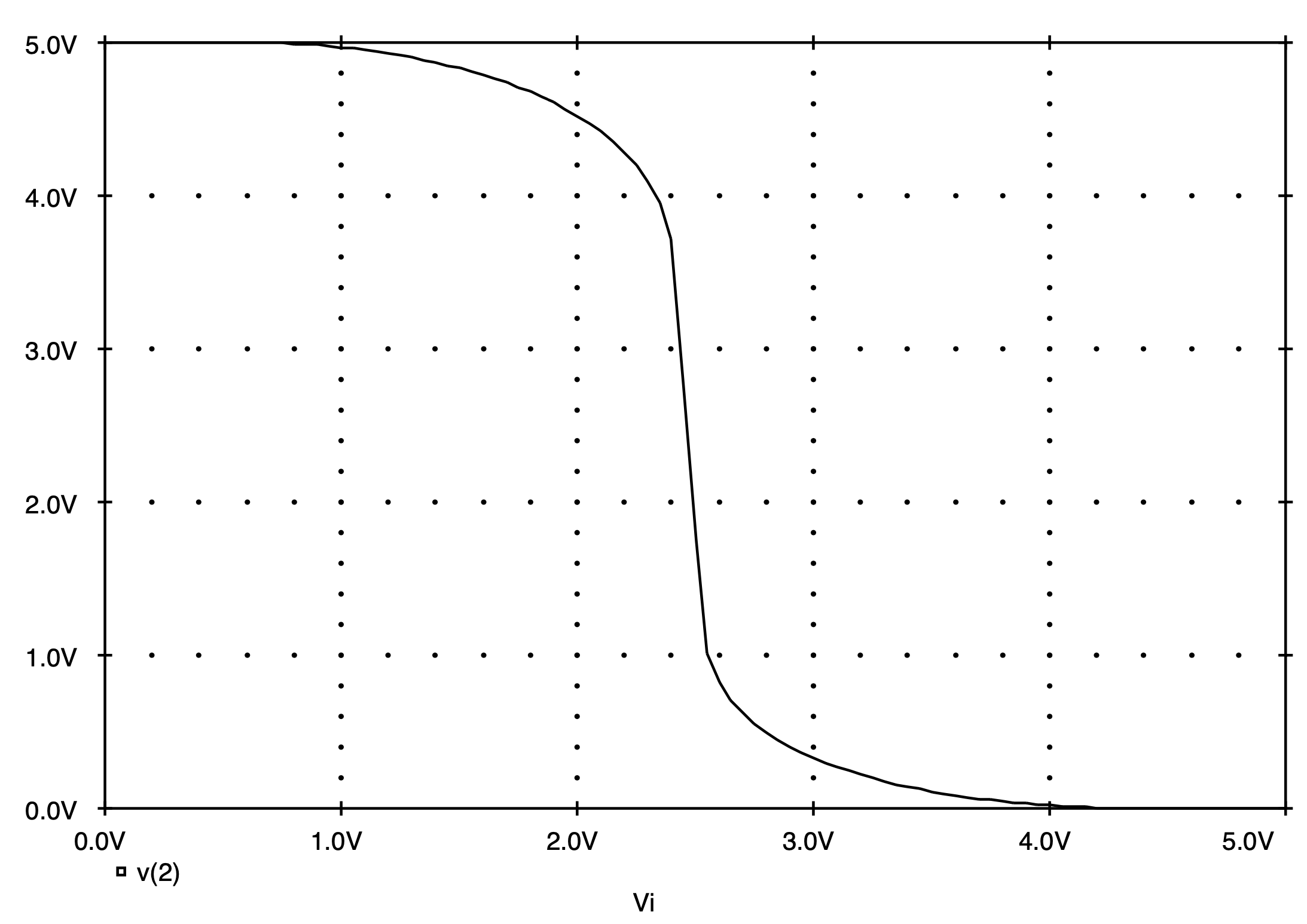
The Spice input file describing the depletion-load inverter circuit of Fig. 13.10 is listed in Fig. 13.11. A DC sweep of the input voltage is requested between 0 V and 5 V. A plot of the output voltage is then requested. In order to compare the results of this analysis with those previously generated for the enhancement-load inverter we have concatenated the two Spice listings shown in Fig. 13.2 and Fig. 13.11 into one input file before submitting the file to Spice for execution.
The results of the two Spice analyses are shown collectively in Fig. 13.12. As is clearly evident, the depletion-load inverter has a steeper transition region than the enhancement-load inverter and therefore approaches more closely the ideal inverter characteristics. As a means of quantifying this we shall compare their respective noise margins.
From Fig. 13.12 we can directly obtain for the depletion-load inverter the output voltage levels VOL and VOH as 0.112 V and 5 V, respectively. To obtain the input threshold levels VIL and VIH, we must determine the input levels (VI) that correspond to dVO/dVI=-1. Following the procedure outlined in the previous section, and with the aid of PROBE, we find VIL=0.845 V and VIH=1.67 V. Thus, the noise margins of the depletion-load inverter are NML=0.733 V and NMH=3.33 V. Both of these values are larger than the corresponding values obtained for the enhancement-load inverter of the previous section; thus, supporting the claim made that the depletion-load inverter behaves more ideally than the corresponding enhancement-load inverter.
|
Fig. 13.13: A CMOS inverter. |
The CMOS Inverter
** Circuit Description ** * dc supplies Vdd 1 0 DC +5V * input digital signal Vi 3 0 DC +5V * MOSFET inverter circuit M1 2 3 0 0 MN L=3um W=3um M2 2 3 1 1 MP L=3um W=9um * BNR 3um transistor model statements (level 3) .MODEL MN nmos level=3 vto=.7 kp=4.e-05 gamma=1.1 phi=.6 + lambda=.01 rd=40 rs=40 pb=.7 cgso=3.e-10 cgdo=3.e-10 + cgbo=5.e-10 rsh=25 cj=.00044 mj=.5 cjsw=4.e-10 mjsw=.3 + js=1.e-05 tox=5.e-08 nsub=1.7e+16 nss=0 nfs=0 tpg=1 xj=6.e-07 + ld=3.5e-07 uo=775 vmax=100000 theta=.11 eta=.05 kappa=1 .MODEL MP pmos level=3 vto=-.8 kp=1.2e-05 gamma=.6 phi=.6 + lambda=.03 rd=100 rs=100 pb=.6 cgso=2.5e-10 cgdo=2.5e-10 + cgbo=5.e-10 rsh=80 cj=.00015 mj=.6 cjsw=4.e-10 mjsw=.6 + js=1.e-05 tox=5.e-08 nsub=5.e+15 nss=0 nfs=0 tpg=1 xj=5.e-07 + ld=2.5e-07 uo=250 vmax=70000 theta=.13 eta=.3 kappa=1 ** Analysis Requests ** .DC Vi 0 5 50mV ** Output Requests ** .PLOT DC V(2) Id(M1) .probe .end
Fig. 13.14: The Spice input file for calculating the input-output voltage transfer characteristics of the CMOS inverter shown in Fig. 13.13. |

|
Fig. 13.15: The input-output voltage transfer characteristic of the CMOS inverter shown in Fig. 13.13.
|
Fig. 13.16: The current in the CMOS inverter versus the input voltage.
|

13.3 The CMOS Inverter
For both custom and semicustom VLSI (very-large-scale-integration), CMOS is generally preferred over all other available technologies. Unlike NMOS technologies, CMOS digital circuits utilize both n-channel and p-channel enhancement-type MOSFETS. An example of a CMOS inverter is shown in Fig. 13.13. In the following we use Spice to compute its voltage transfer characteristics. The n-channel and p-channel MOSFETs will be assumed to be modeled after the same commercial 3 μm CMOS technology used in the previous examples of this chapter. Owning to the fact that the mobility μ for the n-channel device is about 3 times larger than that for the corresponding p-channel device, we shall make the p-channel device 3 times as wide as the n-channel device. Moreover, we shall make the dimensions of the n-channel device equal to the smallest transistor dimensions possible in this technology, i.e., 3 μm by 3 μm.
The Spice input file for the CMOS inverter is shown listed in Fig. 13.14. A sweep of the input voltage level is performed between ground and VDD. The resulting voltage transfer characteristics computed by Spice are shown in Fig. 13.15. Here we see that the output voltage of this gate extends completely between the limits of the two power supply levels. Thus, VOL=0 V and VOH=+5 V. Using the derivative feature of Probe, we find the input logic levels, VIL and VIH, as 2.03 and 2.825 V, respectively. In the case of VIL, we find that the simulated result correlates very closely with that predicted by the simple formula derived in Section 14.5 of Sedra and Smith, 3rd Edition, i.e., VOL= 1/8(3VDD + 2Vtn)= 2.05 V. Similarly, the result predicted by VIH= 1/8(5VDD - 2Vtp) of 2.93 V is quite close to that obtained by simulation. Combining the above results, we find that the high and low noise margins are NMH=2.175 V and MNL=2.03 V, respectively. These noise margins are not equal owning to the fact that M1 and M2 are not exactly matched.
An important attribute of CMOS logic is the fact that the transistors do not conduct any current when settled into a particular logic state. To appreciate this, we plot in Fig. 13.16 the current that flows in the CMOS inverter circuit as a function of the input voltage level. These results indicate that insignificant current flows through the inverter when the input is either smaller than 0.7 V or greater than 4.2 V. We also see that a peak current of 43.8 μA flows through the inverter when the input signal level reaches the midpoint between the voltage supply.
|
Fig. 13.17: A cascade of two CMOS inverter circuits. |
A Cascade Of CMOS Inverters (dynamic effects included)
** Circuit Description ** * dc supplies Vdd 1 0 DC +5V * input digital signal Vi 3 0 DC 1.237 PWL (0,0V 10ns,0V 10.1ns,5V 30ns,5V 30.1ns,0V 50ns,0V) * 1st CMOS inverter M1 2 3 0 0 MN L=3um W=3um M2 2 3 1 1 MP L=3um W=9um Cl1 2 0 0.1pF * 2nd CMOS inverter M3 4 2 0 0 MN L=3um W=3um M4 4 2 1 1 MP L=3um W=9um Cl2 4 0 0.1pF * BNR 3um transistor model statements (level 3) .MODEL MN nmos level=3 vto=.7 kp=4.e-05 gamma=1.1 phi=.6 + lambda=.01 rd=40 rs=40 pb=.7 cgso=3.e-10 cgdo=3.e-10 + cgbo=5.e-10 rsh=25 cj=.00044 mj=.5 cjsw=4.e-10 mjsw=.3 + js=1.e-05 tox=5.e-08 nsub=1.7e+16 nss=0 nfs=0 tpg=1 xj=6.e-07 + ld=3.5e-07 uo=775 vmax=100000 theta=.11 eta=.05 kappa=1 .MODEL MP pmos level=3 vto=-.8 kp=1.2e-05 gamma=.6 phi=.6 + lambda=.03 rd=100 rs=100 pb=.6 cgso=2.5e-10 cgdo=2.5e-10 + cgbo=5.e-10 rsh=80 cj=.00015 mj=.6 cjsw=4.e-10 mjsw=.6 + js=1.e-05 tox=5.e-08 nsub=5.e+15 nss=0 nfs=0 tpg=1 xj=5.e-07 + ld=2.5e-07 uo=250 vmax=70000 theta=.13 eta=.3 kappa=1 ** Analysis Requests ** .TRAN 0.1ns 50ns 0ns 0.1ns ** Output Requests ** .Plot TRAN V(2) V(3) V(4) .probe .end
Fig. 13.18: The Spice input file for computing the transient response for the CMOS inverter cascade shown in Fig. 13.17.
|
|
Fig. 13.19: The transient response of a cascade of two CMOS inverter circuits. The top graph displays the input voltage signal and the bottom graph displays the voltage signals appearing at output of the two inverters. |
Fig. 13.20: The instantaneous power dissipated by the first and second CMOS inverter cascade of Fig. 13.17. The top graph displays the power dissipated by the first inverter and the bottom graph displays the power dissipated by the second inverter.
|


Dynamic Operation
The dynamic operation of a cascade of two CMOS inverters is considered next. The output of each inverter is assumed loaded with a 0.1 pF capacitor to represent the capacitance associated with the interconnect wiring between the two gates. The Spice deck for this particular circuit arrangement is provided in Fig. 13.18. A 0 to 5 V pulse of 20 ns duration is applied to the input of the first inverter circuit. A transient analysis is requested to be performed over a 50 ns interval using a 0.1 ns time step. The voltage at the output of each inverter will be plotted on completion of Spice.
The transient response of the cascade of CMOS inverters as calculated by Spice is presented in Fig. 13.19. The top graph displays the input voltage signal applied to the first inverter and the bottom graph displays the voltage waveform that appears at the output of each inverter circuit. Let us consider the behavior of the voltage signal that appears at the output of the first inverter. Here we see that both the rise and fall time of the output voltage signal are quite similar in duration. With the aid of the Probe facility, we find that the 90% to 10% fall time tTHL is 3.82 ns and the high-to-low input-to-output transition delay tPHL is 2.44 ns. Repeating this for the low-to-high output voltage transition, we find that the 10% to 90% rise time tTLH is 4.17 ns. As well, the low-to-high input-to-output delay tPLH is 2.11 ns. Averaging the above two input-to-output delays, we obtain the propagation time delay tP for the CMOS inverter with a 0.1 pF load to be 2.28 ns.
The voltage waveform appearing at the output of the second inverter is quite similar to that which appears at the output of the first inverter. Using Probe, we find tTHL=3.73 ns, tTLH=3.92 ns, tPHL=2.7 ns and tPLH=2.59 ns. The propagation delay tP is then 2.64 ns. These timing attributes are quite similar to those found for the output voltage waveform associated with the first inverter.
According to hand analysis (see Section 13.5 of Sedra and Smith, 3rd Edition), the expected transitional delays tPHL and tPLH, are found from the following two expressions:
(13.3)
and
(13.4)
Substituting the appropriate parameters obtainable from the Spice deck seen listed in Fig. 13.18, we find tPHL = 0.8 ns and tPLH = 0.88 ns. The propagation delay tP is then 0.84 ns. Comparing these results with those computed by Spice, we find that the results predicted by the above equations underestimate the transition times by about a factor of 3. This is an unreasonably large error. Detailed investigation reveals that the theory used to derive Eqns. (\ref{eqn13.3}) and (\ref{eqn13.4}) assumed that the mobility of each MOSFET (μn and μp) was constant and independent of the voltages that appear at the terminals of the device. Experimental evidence indicates otherwise, and thus a more complicated relationship for the mobility factor has been included in the level 3 MOSFET model of Spice. Through additional simulations and some indirect calculations, it was found for an n-channel MOSFET over a 5 V range of VGS=VDS that μnCOX (kp) varied between 10 μA/V2 and 40 μA/V2. Separately substituting these two extreme values of μnCOX back into Eqn. (\ref{eqn13.3}) indicates that tPHL can range between 0.8 ns and 3.2 ns. When compared to the Spice derived result of 2.7 ns we see that it lies between the two limits predicted by theory.
Similarly, for the p-channel MOSFET we find that μpCOX varies between 4 μA/V2 and 12 μA/V2. Thus, we should expect that the Spice derived transition time tPLH should lie somewhere between 0.86 ns and 2.66 ns. From above, we do indeed see that this is the case, i.e., from Spice, tPLH=2.59 ns.
The instantaneous power dissipated by each CMOS inverter as computed by Spice is shown in Fig. 13.20. The top graph depicts the power dissipated by the first inverter and the bottom graph displays the power dissipated by the second inverter. The shapes of each power waveform are different owing to the different voltage signals that appear at their respective inputs.
|
Fig. 13.21: A two-input CMOS NOR gate.
|
Example 13.3: A Two-Input CMOS NOR Gate
** Circuit Description ** * dc supplies Vdd 1 0 DC +10V * input digital signal Va 4 0 DC 0V Vb 5 0 DC 0V * MOSFET circuit M1 3 5 0 0 nmos_enhancement_mosfet L=3um W=3um M2 3 5 2 2 pmos_enhancement_mosfet L=3um W=12um M3 3 4 0 0 nmos_enhancement_mosfet L=3um W=3um M4 2 4 1 1 pmos_enhancement_mosfet L=3um W=12um * mosfet model statements (by default level 1) .model nmos_enhancement_mosfet nmos (kp=20u Vto=+2V) .model pmos_enhancement_mosfet pmos (kp=10u Vto=-2V) ** Analysis Requests ** .DC Va 0V +10V 50mV ** Output Requests ** .PLOT DC V(3) .probe .end
Fig. 13.22: The Spice input file for calculating the input-output voltage transfer characteristics of the CMOS NOR gate shown in Fig. 13.21.
|

|
Fig. 13.23: The input-output voltage transfer characteristic of the CMOS NOR gate shown in Fig. 13.21 under two different input conditions.
|

13.4 A Two-Input CMOS NOR Gate
An important logic element of digital circuits is the two-input NOR gate shown in Fig. 13.21. Assuming that μCOX of the p-channel MOSFETs is half that of the n-channel MOSFETs at 20 μA/V2 and that the threshold voltage of the PMOS devices is equal but opposite to the Vt of the NMOS device at +2 V, in the following we shall compute the transfer characteristics of this simple gate under the following input conditions: (a) input terminal B connected to ground and (b) input terminals A and B joined together. This same circuit was analyzed by hand by Sedra and Smith in Example 13.3 of their text. Thus, one can compare the results computed here by Spice with those found by hand analysis. Note that the body effect is ignored in this analysis.
We begin our analysis with the Spice input file shown listed in Fig. 13.22. In this particular Spice listing, we have both input signals initially set to 0 V but the voltage at terminal A is varied with the DC sweep command between VDD and ground. The substrate of each device is connected directly to their sources, thereby eliminating their respective body effects.
The results of the Spice simulation are shown in Fig. 13.23. The very sharp, or high gain, transition region is clearly visible with a threshold voltage VTH occurring at 5.53 V. This compares very well with that calculated by hand in Sedra and Smith at 5.31 V.
Also shown in Fig. 13.23 are the computed Spice results of the NOR gate when both input terminals are connected together, and the input voltage is varied between VDD and ground. Here we see that the threshold voltage VTH has shifted down to a level of 4.48 V, which is almost identical to that computed by hand (4.5 V).
When the body effect is included in the analysis, we find very little difference in the results.
|
Fig. 13.24: A set/reset (SR) flip-flop constructed from two cross-coupled NOR gates. Each output of the flip-flop is assumed loaded by a parasitic capacitance of 5 pF.
|
A Set/Reset Flip-Flop
* CMOS NOR GATE subcircuit .subckt NOR_GATE 4 5 3 1 * connections: | | | | * input | | | * input | | * output | * Vdd M1 3 5 0 0 MN L=3um W=3um M2 3 5 2 2 MP L=3um W=18um M3 3 4 0 0 MN L=3um W=3um M4 2 4 1 1 MP L=3um W=18um * BNR 3um transistor model statements (level 3) .MODEL MN nmos level=3 vto=.7 kp=4.e-05 gamma=1.1 phi=.6 + lambda=.01 rd=40 rs=40 pb=.7 cgso=3.e-10 cgdo=3.e-10 + cgbo=5.e-10 rsh=25 cj=.00044 mj=.5 cjsw=4.e-10 mjsw=.3 + js=1.e-05 tox=5.e-08 nsub=1.7e+16 nss=0 nfs=0 tpg=1 xj=6.e-07 + ld=3.5e-07 uo=775 vmax=100000 theta=.11 eta=.05 kappa=1 .MODEL MP pmos level=3 vto=-.8 kp=1.2e-05 gamma=.6 phi=.6 + lambda=.03 rd=100 rs=100 pb=.6 cgso=2.5e-10 cgdo=2.5e-10 + cgbo=5.e-10 rsh=80 cj=.00015 mj=.6 cjsw=4.e-10 mjsw=.6 + js=1.e-05 tox=5.e-08 nsub=5.e+15 nss=0 nfs=0 tpg=1 xj=5.e-07 + ld=2.5e-07 uo=250 vmax=70000 theta=.13 eta=.3 kappa=1 .ends NOR_GATE
** Main Circuit ** * dc supplies Vdd 1 0 DC +10V * input digital signals Vreset 2 0 PULSE (10 0 0 1us 100us 2ms 4ms) Vset 3 0 PULSE (0 10 0 1us 100us 1ms 4ms) * SR Flip-Flop Xnor_gate1 2 5 4 1 NOR_GATE Xnor_gate2 3 4 5 1 NOR_GATE Cp1 4 0 0.1pF Cp2 5 0 0.1pF ** Analysis Requests ** .TRAN 10us 3ms ** Output Requests ** .PLOT TRAN V(4) V(5) .probe .end
Fig. 13.25: The Spice input file for investigating the different states of the SR flip-flop shown in Fig. 13.24.
|

|
Fig. 13.26: The input and output voltage waveforms for the SR flip-flop shown in Fig. 13.24.
|
Fig. 13.27: Determining the minimum time that is required to reset a SR flip-flop when initially in the logic high state. The top graph depicts the reset signal having various pulse widths. The bottom graph shows the response of the flip-flop to the different inputs (Q output).
|


13.4 CMOS SR Flip-Flop
The simplest type of flip-flop is the set/reset (SR) flip-flop shown in Fig. 13.24. It consists of two cross-coupled NOR gates. The output of each gate is loaded with 0.1 pF so as to model the loading effect of other gates connected to the output terminals of the flip-flop. This provides a somewhat realistic situation in which to perform the simulation. In the following, with the aid of Spice, we shall investigate the dynamic behavior of this flip-flop with each NOR gate replaced by a CMOS NOR gate. Each transistor of this NOR gate will be modeled after the commercial 3-micron CMOS transistors used previously in Section 13.3. The Spice description of this flip-flop is provided in Fig. 13.25. Notice that here we have described the two-input CMOS NOR gate as a subcircuit. This simplifies the presentation, and, besides, reduces the amount of typing one has to do to create the Spice input file. By toggling the set and reset input terminals of the flip-flop between VDD and ground, we can observe the storage capability of the flip-flop. This is achieved with the two input source PULSE statements.
The results of this analysis are shown in Fig. 13.26. The top two waveforms are the SET and RESET voltage waveforms appearing at the inputs to the flip-flop. The bottom two waveforms Q and Q-bar are the signals appearing at the flip-flop outputs. Clearly, when the SET input is high and the RESET input is low, the output Q goes high and Q-bar goes low. This condition remains when both SET and RESET are low. However, we see from the simulated results that when RESET goes high and SET remains low, the two outputs change state.
As a matter of practical consideration when working with a SR flip-flop, one is sometimes faced with the question of what is the minimum time required to reset the flip-flop (tRESETmin). This can easily be answered with the aid of Spice. Consider initializing the state of the flip-flop such that Q is logically high, and Q-bar is logically low. This is simply achieved by using the following initial condition (.IC) statement:
.IC V(4)=+10V V(5)=0V
Further, by adjusting the duration of a pulse applied to the RESET input of the flip-flop we can find the input condition which no longer resets the flip-flop. This will then indicate the minimum time required to reset the flip-flop. Let us begin our investigation with an input pulse of 5 ns duration, then check the state of the flip-flop. If the Q output of the flip-flop settles into the logic low state, then tRESETmin is probably something less than this value. We will then proceed to decrease this value by 0.5 ns and re-simulate the circuit to see whether the flip-flop has been reset. If, once again, this is not the case, then we keep repeating this process until we find the duration of the input pulse that will not reset the flip-flop.
Beginning our analysis with a pulse having a 5 ns duration was based on the time required for a logic signal to propagate around a loop of two NOR gates. As a rough estimate of the time required for a signal to propagate through two NOR gates, let us consider that the propagation time of a NOR gate is about the same as that for an inverter circuit of similar dimensions. Recall that we found the propagation time for a CMOS inverter in Section 13.3 to be 2.28 ns. Thus, we can expect tRESETmin to be about 4.56 ns. Thus, to ensure that our starting point is one that resets the flip-flop, we shall begin our analysis with a pulse of 5 ns duration.
Our analysis will make use of the same Spice deck used previously for this flip-flop (seen listed in Fig. 13.25). We shall simply modify the two input signal sources as follows:
|
Vreset 2 0 PWL (0s,0V 1ns,0V 1.1ns,10V 5ns,10V 5.1ns,0V 15ns,0V) Vset 3 0 DC 0
|
As well, we shall modify the analysis request as follows,
.TRAN 0.1ns 15ns 0 0.1ns.
In addition to a pulse input of 5 ns duration, we shall also concatenate together two other similar Spice decks having input pulses of 4.5 ns and 4 ns duration.
On completion of the Spice analysis, we find the Q output of the flip-flop shown in Fig. 13.27 for the three different input conditions. For an input reset signal of 5 or 4.5 ns duration, we see that the flip-flop changes state. But, for an input signal of 4 ns duration, we see that the flip-flop begins to change state, but then returns back to the high state. Thus, we can conclude that the minimum time to reset the flip-flop is greater than 4 ns but less than 4.5 ns. We could do more refinement of this search process if it was thought necessary, but we will, at this time, be content with tRESETmin=4.5 ns.
|
Fig. 13.28: A cascade of two DCFL GaAs inverter circuits with the first gate loaded with 30 fF.
|
Example 13.4: A DCFL GaAs Gate
** Circuit Description ** * dc supplies Vdd 1 0 DC +1.5V * input signal Vi 3 0 PWL (0,0V 1ns,0V 1.1ns,700mV 3ns,700mV 3.1ns,0V 5ns,0V) * amplifier circuit B1 2 3 0 enchancement_n_mesfet 50 B2 1 2 2 depletion_n_mesfet 6 Cp1 2 0 30fF B3 4 2 0 enchancement_n_mesfet 50 B4 1 4 4 depletion_n_mesfet 6 * mesfet model statements (by default, level 1) .model enchancement_n_mesfet gasfet (beta=0.1m Vto=+0.2V lambda=0.1 + n=1.1 Is=5e-16 Cgd=1.2e-15 Cgs=1.2e-15 Rs=2500) .model depletion_n_mesfet gasfet (beta=0.1m Vto=-1.0V lambda=0.1 + n=1.1 Is=5e-16 Cgd=1.2e-15 Cgs=1.2e-15 Rs=2500) ** Analysis Requests ** .DC Vi 0V 0.8V 10mV .TRAN 0.1ns 5ns 0s 0.1ns ** Output Requests ** .PLOT DC V(2) .PLOT TRAN V(2) .probe .end
Fig. 13.29: The Spice input file for calculating the input-output transfer characteristics and the pulse response of the DCFL inverter circuit shown in Fig.13.28.
|

|
Fig. 13.30: The input-output voltage transfer characteristics for the DCFL inverter circuit shown in Fig. 13.28.
|
Fig. 13.31: The transient response behavior of the DCFL inverter circuit shown in Fig. 13.28 subject to a 2 ns wide input pulse signal with 100 ps rise and fall times.
|


13.5 A Gallium-Arsenide Inverter Circuit
As an emerging IC technology, GaAs shows promise for high-speed electronic design. In Fig. 13.28 we present an inverter circuit in this technology, known as the direct-coupled FET (DCFL) inverter. Specifically, two inverter circuits are connected in cascade with a 30 fF lumped capacitor representing the distributed capacitance of the wiring that interconnects the two inverters. The lower two MESFETs of each inverter, B1 and B3, are enhancement MESFETs and their corresponding loads, B2 and B4, are depletion MESFETs. We shall assume that the parameters describing these two types of MESFETs per micron width are as follows: L=1 μm, VtD=-1 V, VtE=0.2 V, b=0.1 mA/V2, and lambda=0.1 V-1. Moreover, in order to model the behavior of the Schottky diode that makes up the gate to source region of each MESFET, we shall set n=1.1 and IS=5 ´ 10-16 A. The capacitive effects of each transistor will be modeled using Spice parameters CGS=1.2 ´ 10-15 F and CGD=1.2 ´ 10-15 F. Let the width of the input MESFET of each inverter be 50 μm, and let the width of the load MESFETs be 6 μm.
Using Spice, we shall compute the voltage transfer characteristics of the first inverter with the second inverter present. As well, we shall compute the transient response of the first inverter for a 2 ns duration pulse input.
With the Spice deck provided in Fig. 13.29, the input-output voltage transfer characteristics for the DCFL inverter shown in Fig. 13.30 was calculated. Using Probe, we find that VOH=708 mV, VOL=247 mV, and by taking the derivative of the output voltage with respect to the input voltage, we find VIH=651 mV and VIL=491 mV. Therefore, the low and high noise margins are 245 mV and 56.7 mV, respectively. Here we see that the high noise margin appears quite low, a disadvantage of this type of logic gate. Nevertheless, these gates are presently receiving considerable attention in the development of GaAs digital circuits owing to their simplicity and low power dissipation.
The transient response of the DCFL inverter circuit is shown in Fig. 13.31 for a 2 ns duration pulse having a voltage swing between ground and VOH. The input pulse has an assigned rise and fall time of 100 ps. The output response has an unsymmetrical rise and fall time of 623.5 ps and 337 ps, respectively. The two propagation delays tPHL and tPLH are found to be 198 ps and 211 ps, respectively. Thus, the average propagation delay of this particular DCFL inverter gate is 204.5 ps.
13.6 Spice Tips
· The derivative dVO/dVI can be computed using the derivative command of Probe. A plot of VO versus VI must first be computed using the DC sweep command.
13.7 Problems
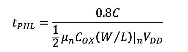
13.1. An n-channel enhancement MOS device, used in an inverter load operating from a 5 V supply, has Vto ranging from 1 to 1.5 and gamma ranging from 0.3 to 1 {V1/2} and 2ff=0.6 V. What is the lowest value of VOH that will be found using transistors of this kind?
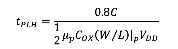
13.2. With the aid of Spice, determine the average propagation delay, the average power dissipation, and the delay-power product of an inverter for the following conditions:
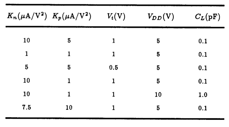
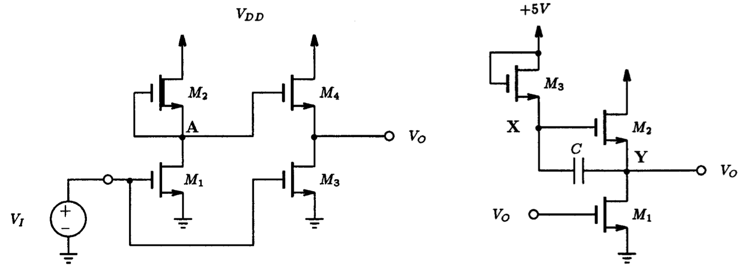
Fig. P13.3. Fig. P13.4
13.3. The circuit shown in Fig. P13.3 can be used in applications, such as output buffers and clock drivers, where capacitive loads require high current-drive capability. Let VtE=1 V, VtD=-3 V, VDD=5 V, μnCOX=20 μA/V2, W1=W2=12 μm, L1=L2=L_3=L_4=6 μm. W3=120 μm, and W4=240 μm.
(a) Find VAH, VOH, VAL and VOL for VI (high) = 5 V. Note that VAH denotes the high level at node A, etc.
(b) Find the total static current with the output high and the output low.
(c) As VO goes low, find the peak current available to discharge a load capacitance C=10 pF.
(d) Also, find the discharge current for VO at 50% output swing point and thus find the average discharge current and tPHL.
(e) Repeat (c) for VO going high, thus finding tPLH.
13.4. The circuit shown in Fig. P13.4, called a bootstrap driver, is intended to provide a large output voltage swing and high output drive current with a reasonable standing current. Let VDD=5 V, Vt=1 V, μnCOX|1=40 μA/V2, μnCOX|2=10 μA/V2, μnCOX|3=1 μA/V2, and assume C=10 pF. With the aid of Spice, answer the following questions:
(a) Find the voltages at node X and Y when VI has been high (at 4 V) for some time.
(b) When VI goes low to 0 V and Q1 turns off, to what voltages do nodes X and Y rise?
(c) Find the current available to charge a load capacitance at Y as soon as VI goes low and Q1 turns off.
(d) As VI goes high again, what current is immediately available to discharge the load capacitance at Y.
(e) What is the current shortly thereafter, when vY=4 V?
13.5. A particular CMOS inverter uses n- and p-channel devices of identical sizes. If μnCOX=2μpCOX=10 μA/V2, |Vt|=1 V, and VDD=5 V, find VIL and VIH and hence the noise margins.
13.6. For a CMOS inverter having Vtn=-Vtp=1 V, VDD=5 V, μnCOX=2μp COX=20 μA/V2, (W/L)n=10 μm/5 μ{m}, and (W/L)p=20 μm/5 μm, determine using Spice, what the maximum current that the inverter can sink with the output not exceeding 0.5 V? Also find the largest current that can be sourced with the output remaining within 0.5 V of VDD.
13.7. For an inverter with μnCOX=2μp COX=50 μA/V2, Vtn=-Vtp=0.8 V, VDD=5 V, (W/L)n=4 μm/2 μm, and (W/L)p=8 μm/2 μm, using Spice, find the peak current drawn from a 5 V supply during switching.
13.8. If the inverter specified in Problem 13.7 is loaded with a 0.2 pF capacitance, determine, using Spice, the dynamic power dissipation when the inverter is switched at a frequency of 20 MHz. What is the average current drawn from the power supply?
13.9. For a CMOS inverter having Vtn=-Vtp=2 V, VDD=5 V, μnCOX=2μpCOX=50 μA/V2, and loaded with a 0.1 pF capacitance. If the inverter is to be clocked at 100 MHz, determine the values of (W/L) that will result in a delay-power product no larger than 0.1 pJ. Verify that this is indeed the case using Spice.
13.10. Consider a DCFL gate fabricated in GaAs technology for which L=1 μm, VtD=-1 V, VtE=+0.2 V, and lambda=0.1 V-1, and let VDD=1.5 V. Determine the widths of the two MESFETs that yields a NMH=0.2 V. Verify your choice using Spice. What is the resulting value of NML?