Chapter 3
Diodes
Gordon W. Roberts
Department of Electrical & Computer Engineering, McGill University
The most fundamental nonlinear element of electronic circuits is the semiconductor junction diode. Because of its importance in both discrete and integrated circuits, the creators of Spice have made provisions for a built-in model of the semiconductor diode. In this chapter we shall outline how to access the diode model, and how to alter the model parameters to suit particular applications. Finally, using Spice, we shall investigate the behavior of some commonly used diode circuits, and compare the results with those obtained through the approximate hand analysis methods.
3.1 Describing Diodes to Spice
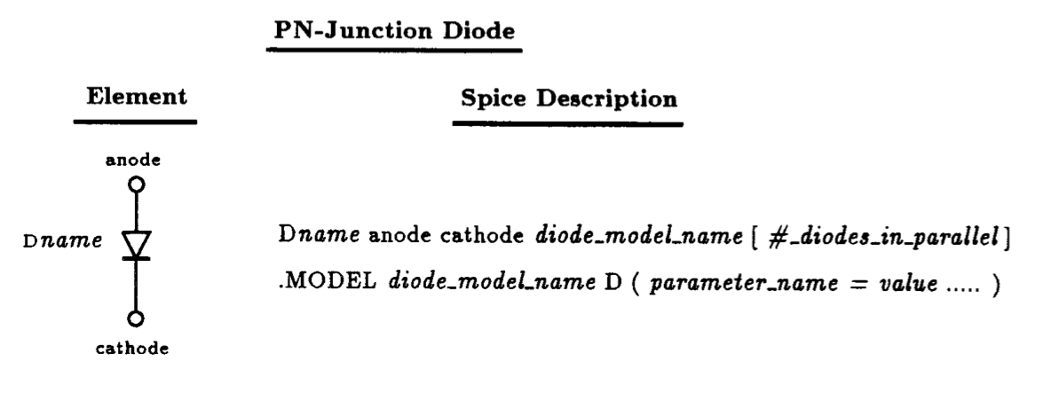
A pn junction diode is described in the Spice Description Language (SDL) using two statements. One statement is necessary to specify the diode type and the manner in which it is connected to the rest of the network, and the other statement is required to specify the values of the parameters of the built-in model for the diode type specified by the first statement. In the following we shall describe these two statements.
3.1.1 Diode Element Description
The presence of a pn junction diode in a circuit is described in SDL using an element statement beginning with the letter D. If more than one diode exists in a circuit, then a unique name must be attached to D to uniquely identify each diode. This is then followed by the two nodes that the anode and cathode of the diode are connected to. Subsequently, on the same line, the name of the model that will be used to characterize this particular diode is given. The name of this model must correspond to the name given on a model statement containing the values of the model parameters. Lastly, one has the option of specifying the number of diodes that are considered to be connected in parallel. This acts as a convenient way of scaling the cross-sectional area of the device.
For quick reference, we depict in Fig. 3.1 the syntax of the Spice statements pertaining to the pn junction diode. We shall discuss the model statement more fully next.
|
Fig. 3.1: Spice element description for the pn junction diode. Also listed is the general form of the associated diode model statement. A partial listing of the parameter values applicable to the pn junction diode is given in Table 3.1.
|
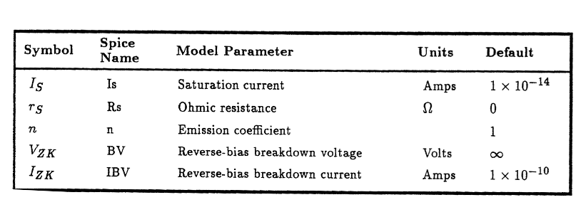
Table 3.1: A partial listing of the Spice parameters for a static pn junction diode model.
|
3.1.2 Diode Model Description
As is evident from Fig. 3.1, the model statement for the pn junction begins with the keyword .MODEL and is followed by the name of the model used by a diode element statement, the letter D to indicate that it is a diode model, and a list of the values of the model parameters (enclosed between brackets). There are quite a few parameters associated with the pn junction diode model used by Spice, and their individual meanings are rather involved. Instead of trying to describe the meaning of every parameter, we shall only consider here the parameters of the Spice diode model that are relevant to our introductory study of diodes in this chapter.
|
Fig. 3.2: The Spice large-signal pn junction diode model.
|
Fig. 3.3: A small-signal equivalent circuit used by Spice to represent a semiconductor diode.
|


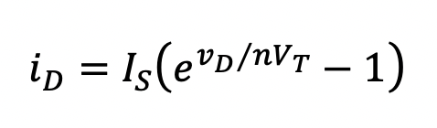
The large-signal model used for the semiconductor junction diode in Spice is shown in Fig. 3.2. The DC characteristic of the diode is modeled by the nonlinear current source iD which depends on vD according to the following equation:
(3.1)
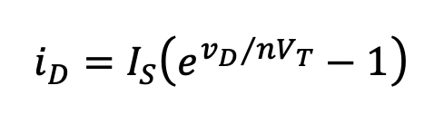
Here IS, n and VT are device parameters: IS is referred to as the saturation current, n the emission coefficient, and VT as the thermal voltage. Both IS and n are related to the physical make-up of the diode, in contrast to the thermal voltage VT which depends on the temperature of the device and two physical constants, i.e.,
(3.2)

Here k is Boltzmann's constant (k=1.381 x 10⁻²³ V C/°K), T is the absolute temperature in degrees Kelvin, and q is the charge of an electron (q=1.602 x 10⁻¹⁹). In many approximate analyses, VT is assumed to equal 25 mV at a room temperature of 290 °K. However, Spice does not approximate this quantity, and instead uses the exact values of k, T and q to determine VT.
Finally, the series resistance rS in the diode model shown in Fig. 3.2 simply models the lump resistance of the silicon on both sides of the semiconductor junction. The value of rS may range from 10 to 100 W in low-power diodes.
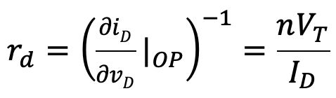
Under small-signal conditions, Spice adopts the diode equivalent circuit shown in Fig. 3.3. Here rd is the incremental resistance of the diode around its quiescent operating point and is expressed in terms of the DC bias current ID as follows:
(3.3)
LTSpice does not use the name rd for the small-signal resistance of the diode, instead it refers to this resistance in the Spice Error Log file as Req.
Under large reverse-bias conditions (i.e., vD << 0), the operation of the semiconductor diode is dominated by physical effects other than those which give rise to Eqn. (3.1). More specifically, under large reverse-bias conditions, the semiconductor diode enters its breakdown region and begins to conduct a large reverse current. In Spice, the dependence of this reverse current on reverse voltage is modeled as an exponential function - much like that of the forward bias region. In fact, for voltages below a commonly specified reverse-bias voltage -VZK (breakdown voltage) the i-v characteristic is a near vertical straight line. Correspondingly, at this breakdown voltage -VZK, the diode is said to conduct a reverse current of -IZK. Thus, VZK and IZK specify the start of the breakdown region of the semiconductor diode. Note that these two quantities are positive numbers.
A partial listing of the parameters associated with the Spice pn junction diode model under static conditions is given in Table 3.1. The first column lists the symbol used to denote each parameter as described in this chapter. The next column lists the corresponding name of the parameter used by Spice; this is the only name that can be used for this parameter in the list of model parameters on a .MODEL statement. Also listed are the associated default values which the parameter assumes if a particular value is not specified on the .MODEL statement. To specify a parameter value one simply writes, for example, Is=1e-13, n=2, BV=50, IBV=1e-12, etc.
|
(a)
(b)
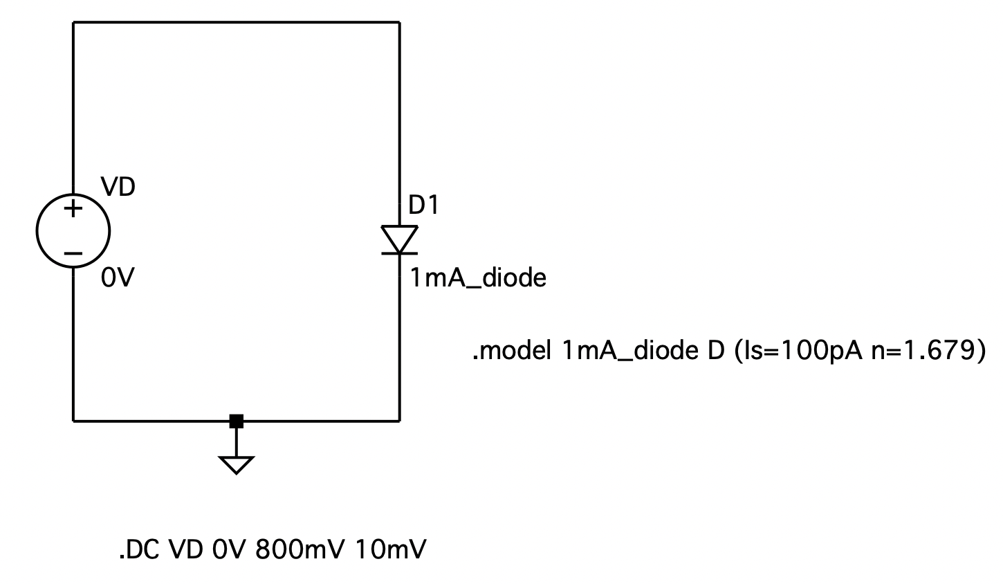
Fig. 3.4: (a) Simple circuit arrangement for determining the i-v characteristic of a 1 mA diode. (b) Circuit schematic captured by LTSpice along with its various Spice directives.
|
LTSpice As A Curve Tracer: Diode I-V Characteristics * * Circuit Description * VD N001 0 0V D1 N001 0 1mA_diode * * diode model statement * .model 1mA_diode D (Is=100pA n=1.679) * * unused diode statements * .model D D .lib/Users/roberts/Library/Application Support/LTspice/lib/cmp/standard.dio * * Analysis Requests * .DC VD 0V 800mV 10mV .backanno .end
Fig. 3.5: Circuit netlist for determining diode forward-bias characteristics.
|

|
Fig. 3.6: Forward-bias characteristics of a 1 mA diode with an emission coefficient of 1.679; upper curve: linear scale, lower curve: semilogarithmic.
|

3.2 LTSpice as a Curve Tracer
Whenever a model of a device is created, whether it be a model of an op-amp, diode or some other electronic device, one should make certain the expected terminal characteristics are actually captured by the model. In the laboratory, a curve tracer is an instrument that is commonly used to measure the DC terminal characteristics of semiconductor devices. Using LTSpice, we can emulate the behavior of the curve-tracer and therefore determine whether the DC model chosen to represent the diode is suitable.
A curve-tracer is an instrument designed to measure the i-v characteristics of semiconductor devices over a wide range of voltage and current levels. A typical curve-tracer instrument contains a set of variable voltage and current sources that are capable of varying their level beginning at some lower value and proceeding to some maximum value in discrete steps. Concurrently, the current supplied to - or the voltage that develops across - the externally attached device is measured and recorded. On completion, the results are displayed on the screen of a cathode ray tube (CRT) as a graph. To emulate this behavior using Spice we make use of the DC sweep command in conjunction with some DC source.
For example, in Fig. 3.4 we display a voltage source (VD) with a single diode Dtest as its load. We shall assume that the diode is a ``1 mA diode’’ (meaning that it conducts a current of 1 mA at a forward bias voltage of 0.7 V) and that its voltage-drop changes by 0.1 V for every decade change in current. Thus, using the diode current equation listed in Eqn. (3.1), one can show that this diode is characterized by IS=100 pA and n=1.679. To describe this particular 1 mA diode to LTSpice, we use the following model statement:
.model 1mA_diode D (Is=100pA n=1.679).
This model statement will be added to the schematic of the diode circuit using the Spice Directive command in much the same way a subcircuit statement was added in the previous chapter. Now, to compute and display the forward-bias i-v characteristics of this 1 mA diode we shall sweep VD in Fig. 3.4 from 0 V to 800 mV in 10 mV steps. This is achieved by including the following DC sweep command on the schematic:
.DC VD 0V 800mV 10mV
The circuit schematic and its directives as captured by LTSpice are shown in the diagram of Fig. 3.4(b). The circuit netlist generated by LTSpice (with some rearrangements and comments added for clarity) can be seen listed in Fig. 3.5. Of particular note is that extraneous diode-related statements:
|
.model D D .lib/Users/roberts/Library/Application Support/LTspice/lib/cmp/standard.dio
|
These are default statements added with the initial inclusion of the diode D dropped onto the schematic. The model statement defines the diode model and the lib statement points to a file in the LTSpice directory containing the parameters of the diode. As the model name for the diode was changed from D to 1mA_diode, these two statements will have no effect on the analysis.
On execution and selection of the diode current, the i-v characteristic for this particular diode is shown in Fig. 3.6 in two different forms. The top curve displays the diode i-v characteristic on a linear scale, whereas the bottom curve is on a semi-logarithmic scale. It is immediately obvious how linear the i-v characteristic is on a semi-log scale.
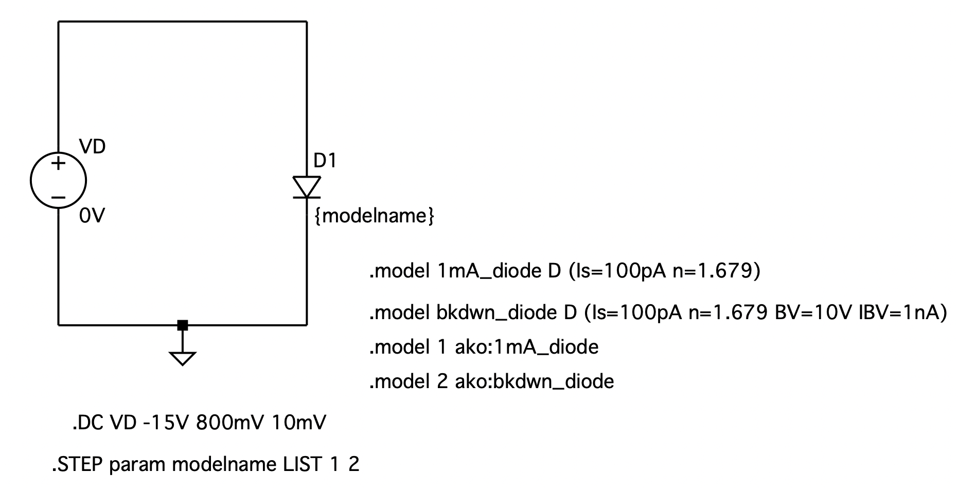
Both the forward and reverse-bias of this diode can plotted by sweeping the DC voltage over the negative voltage region from -15 V to 800 mV. To compare this behavior with another diode characteristics, say one with a breakdown region defined by VZK=10 V and IZK=1 nA, one can add another diode model, say as follows
.model bkdwn_diode D (Is=100pA n=1.679 BV=10V IBV=1nA).
and re-run the LTSpice analysis. However, the results would appear on a separate graph. This would make comparison difficult. A better way is to replace the diode model name by a general variable, say modelname, enclosed in brackets as {modelname} to invoke replacement before Spice execution. Next, using the .STEP directive, assign the modelname a list of possible model names, such as
.STEP param modelname 1mA_diode bkdwn_diode
The intent is to cycle through the list of model names and evaluate the circuit behavior using different diode models. Unfortunately, the .param function of LTSpice only wants to work with numbers, not names. So one could rename the diode models with numbers and then run the .STEP command. However, this would make the diode models less meaningful to the user. Instead, LTSpice provides a means to alias a name with a number using the ``ako’’ option. The ako is a short form for ``a kind of.’’ Here’s how this aliasing feature would work with the two diode models:
|
.model 1mA_diode D (Is=100pA n=1.679) .model 1 ako:1ma_diode
.model bkdwn_diode D (Is=100pA n=1.679 BV=10V IBV=1nA) .model 2 ako:bkdwn_diode |
Updating the schematic in the command window as shown in Fig. 3.7 and executing LTSpice, results in the comparison plot shown in Fig. 3.8 for the two diode models. Clearly, both these diodes have identical forward-bias characteristics but very different reverse-bias behavior.
|
Fig. 3.7: Demonstrating the LTSpice circuit schematic setup for simulating a circuit with different device models.
|
Fig. 3.8: Comparing the i-v characteristic of a 1 mA diode with a breakdown region specified by VZK=10 V and IZK=1 nA, and one that has no breakdown region specified.
|

3.2.1 Extracting the Small-Signal Diode Parameters
If an operating point (.OP) analysis directive is specified, then the small-signal parameters of each diode within the circuit captured by LTSpice will be listed in the output file. For example, the small-signal parameters of the 1 mA diode used in the above example biased at 700 mV would be found in the Spice Error log file as follows:
|
Semiconductor Device Operating Points: --- Diodes --- Name: d1 Model: 1ma_diode Id: 1.00e-03 Vd: 7.00e-01 Req: 4.34e+01 CAP: 0.00e+00 |
Included in this list of operating point information is the name of the diode assigned by the user and the name of the model used to characterize the diode. This is followed by the DC bias point information, ID and VD, and then, the incremental resistance of the diode REQ. At the bottom of this list is the small-signal capacitance CAP associated with this diode. We shall defer discussion of this parameter until Chapter 7.
At this point it would be highly instructive to check that the small-signal resistance of the diode computed by Spice in the list of operating point information agrees with that computed by the simple formula rd = nVT/ID. Consider, for this particular diode, n=1.679, VT=25.8 mV and ID=1 mA. Thus, on substituting these values into the expression for rd, we get 43.47 Ω, almost in perfect agreement with the value computed by Spice (43.4 Ω).
|
|
|
Table 3.2: The general syntax of the Spice command for setting the temperature of a circuit.
|

3.2.2 Temperature Effects
To investigate the effect of temperature variation on diode behavior we simply repeat the above curve-tracer analysis at different temperatures. To accomplish this, one just adds a .TEMP statement with the temperature (in degrees Celsius) at which the analysis should be performed. If more than one temperature is listed, then the analysis will be repeated for each temperature. A general description of the syntax of this command is provided in Table 3.2. For the example above, let us compute the diode i-v characteristics for temperatures of 0°, 27° and 125°C. The statement that should be added to the schematic in the command window shown in Fig. 3.4 is:
.TEMP 0 27 125.
The LTSpice job is then re-run and the results are shown in Fig. 3.9. The results displayed in this graph were restricted to lie within a 0 to 1 mA current range by adjusting the scale of the y-axis. This was deemed necessary in order to best illustrate the diode characteristics for all three temperatures on one graph. It should be evident from Fig. 3.8 that as the temperature increases the i-v curve for the diode shifts to the left. Close scrutiny using the cursor facility of the waveform viewer (move the mouse to the trace label at the top of the screen and double-click the left mouse button) reveals that for a constant current of 0.4 mA the forward diode voltage decreases by about 1.7 mV for every degree C increase in temperature.
|
Fig. 3.9: Illustrating the temperature dependence of the forward bias characteristics of a 1 mA diode.
|
Fig. 3.10: i - v characteristics of a near-ideal diode.
|


3.3 Approximating Ideal Diode Behavior
The ideal diode concept often simplifies the analysis of electronic circuits containing diodes by assuming that the forward bias voltage across a conducting diode is zero regardless of the level of current flowing through it, and conversely, when in the blocking state, it prevents current from flowing through it regardless of the level of reverse bias voltage appearing across it. An ideal model for a diode does not exist in Spice for the simple reason that an ideal diode does not exist in practise. However, there are numerous occasions when an ideal diode is useful to have; especially when attempting to represent an arbitrary nonlinear function.
Consider the equation for the static diode current given in Eqn. (3.1) and repeated below for convenience,
There are two parameters associated with this equation that are under our direct control: the saturation current IS and the emission coefficient n. Our problem is to adjust one, or both, of these parameters, such that (a) vD tends towards zero when the diode is considered on, and (b) iD tends towards zero when it is considered off. On examination of Eqn. (3.1) we see that condition (b) is satisfied when IS is reduced and/or n is increased (recall that vD is negative). Conversely, from the equation depicting the diode voltage (a simple re-arrangement of Eqn. (3.1)),
(3.4)
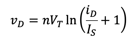
we see that alterations will tend to increase vD under forward bias condition instead of reducing it. This suggests that conditions (a) and (b) cannot both be met simultaneously by adjusting either IS or n. We notice from Eqn. (3.1), however, that under reverse bias conditions that regardless of the value of n, iD will never exceed IS - a near-zero value. Thus, a good approximation to ideal diode behavior is obtained by making n small because this will reduce the diode forward voltage drop and maintain low reverse-bias current. Experience has shown that a value for n between 0.01 and 0.001 works well. Values smaller than 0.001 usually result in DC convergence problems. Fig. 3.10 illustrates the i-v characteristics of a simple diode characterized by the following model statement:
.model ideal_diode D (Is=100pA n=0.01).
For all intents and purposes, the curve shown in Fig. 3.10 is an excellent representation of ideal diode behavior.
|
(c)
Fig. 3.11: (a) A 2.1 V voltage regulator circuit consisting of three diodes in series. (b) Representing the power supply fluctuation with a 60 Hz, 1 V-peak sinusoidal signal superimposed on a constant DC voltage of +10 V. (c) Circuit captured by LTSpice with model descriptions and Spice directives given.
|
A Three Diode String Voltage Regulator Circuit
* * Circuit Description * Vps PS 0 10V Vripple PSwRipple PS SINE(0 1V 60Hz) * D1 OUT N001 reg_diode D2 N001 N002 reg_diode D3 N002 0 reg_diode R1 PSwRipple OUT 1k Rload OUT 0 {Rload} * * diode model statement .model reg_diode D (Is=831.5pA n=2) * * unused diode statements * .model D D .lib /Users/roberts/Library/Application Support/LTspice/lib/cmp/standard.dio * * Analysis Requests * .TRAN 0.5ms 100ms 0ms 0.5ms .STEP param Rload LIST 1000Meg 1k .backanno .end
Fig. 3.12: The LTSpice netlist for computing the time-varying output voltage of the voltage regulator circuit shown in Fig. 3.10. |


3.4 Voltage Regulation Using a String of Diodes
Connecting one or more diodes in series with a resistor and a power supply provides a simple means of creating a relatively constant voltage, somewhat independent of fluctuations in the power supply level. One example of this is demonstrated in Fig. 3.11(a) where three diodes and a 1 k-Ω resistor are connected in series with a +10 V DC voltage source. Since the forward voltage drop of each diode remains almost constant at approximately +0.7 V for a wide range of diode currents, the voltage that appears at the output of this regulator circuit is about +2.1 V. With the aid of LTSpice, we would like to investigate the effect of the fluctuations in the +10 V supply on the output voltage. We shall assume that the fluctuations are caused by a 60 Hz, 1 V-peak sinusoidal signal riding on the +10 V DC voltage level. This arrangement is illustrated in part (b) of Fig. 3.11. In addition, the voltage regulator will be assumed to be loaded with a 1 kΩ load. The effect of this load on the unloaded regulator will be investigated by assigning the load a variable {Rload} and stepping through a very large load of 100 MΩ (essentially no-load), followed by a 1 kΩ load. This is easily achieved by typing the following. STEP command in the LTSpice command window:
.STEP param Rload LIST 1000Meg 1k
A transient analysis is requested to compute the behavior of this regulator circuit over six periods of the 60 Hz input signal. On average, 33.3 points-per-period of the input signal (i.e., a sampling interval of 0.5 ms) are to be collected. This will provide enough points so that a smooth graph of the output waveform can be plotted. The corresponding LTSpice captured circuit with the above-mentioned directives are shown in Fig. 3.11(c). In Fig. 3.12 we list the circuit netlist for this circuit as generated by LTSpice. The results shown there confirm what was specified by the schematic Spice directives. Once the LTSpice results are obtained, we shall compare them with those obtained by hand.
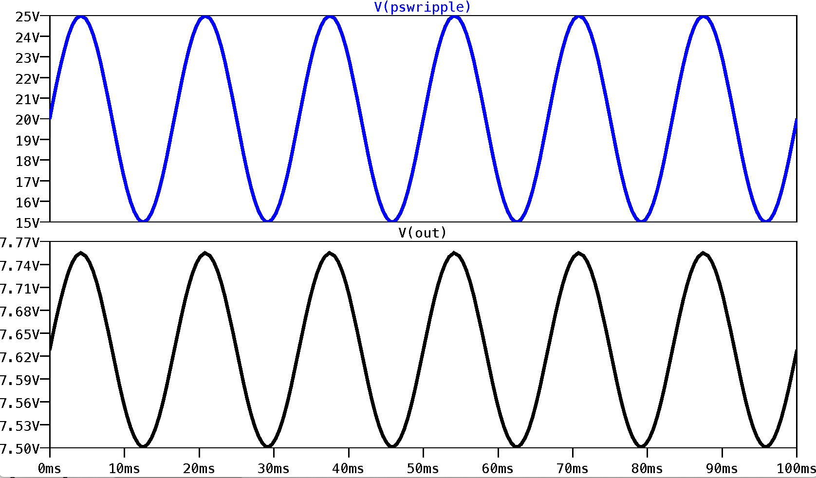
On completion of the transient analysis, the output waveforms from the voltage regulator circuit are shown in Fig. 3.13. The bottom curve is the output voltage waveform of the regulator circuit having a 1 kW load, and the curve above it is the output voltage signal of the regulator circuit under no-load conditions. As is evident, the output voltage waveform from the unloaded regulator circuit is sinusoidal, having the same frequency as the power supply fluctuations (60 Hz). It has an average value of 2.486 V, slightly different from that estimated above (2.1 V) assuming the voltage drop of each diode is 0.7 V. The peak-to-peak excursion of this output voltage signal is found using the cursor facility of the waveform viewer to be 40.7 mV. This is obviously much less than the peak-to-peak excursions of the power supply fluctuations of 2 V. In the case of the loaded regulated circuit, we see that the output voltage signal is riding on a DC level of 2.426 V, a decrease in the DC level of 60 mV below that of the unloaded regulator circuit. The peak-to-peak amplitude of the ripple superimposed on the output voltage is found to have increased to 57.1 mV.
|
|
|
Fig. 3.13: The output voltage signals from the three-diode string voltage regulator shown in Fig. 3.10 assuming that the power supply voltage varies sinusoidally with an amplitude of 1 V. The bottom waveform is the output of the regulator with a 1 kW load and the one above it is with no load.
|

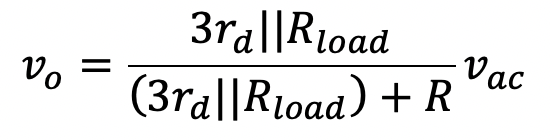
According to small-signal analysis, the expected output voltage ripple of the unloaded diode regulator circuit subject to power supply fluctuations vac is simply given by the following expression:
(3.5)
![]()
where rd is the incremental resistance of each diode. To obtain the small-signal parameters of each diode, set the load to 100Meg to act as the unloaded condition, and replace the transient analysis with an .OP directive. On doing so, the diode small-signal parameters for the unloaded case are found to be
|
--- Diodes --- Name: d3 d2 d1 Model: reg_diode reg_diode reg_diode Id: 7.51e-03 7.51e-03 7.51e-03 Vd: 8.29e-01 8.29e-01 8.29e-01 Req: 6.88e+00 6.88e+00 6.88e+00 CAP: 0.00e+00 0.00e+00 0.00e+00 |
As is evident, each diode has an incremental resistance (rd) of 6.88 Ω. Interestingly enough, this is quite close to the value predicted by simple hand analysis at 6.3 Ω; a result obtained by assuming a 0.7 volt-drop across each diode leading to a diode current of 7.9 mA. Substituting, rd=6.88 Ω into Eqn. (3.5) above, and assuming a 2 V peak-to-peak input signal, results in an estimated output peak-to-peak voltage signal of 40.4 mV: very close to the value of 40.7 mV found by LTSpice.
In the case of the 1 k-Ω loaded regulator circuit, hand analysis also leads to a similar confirmation. Small-signal analysis of the three-diode regulator circuit with a 1 k-Ω load leads to an output voltage given by the expression:
(3.6)
Substituting the appropriate circuit parameters, together with the incremental resistance of each diode as calculated by LTSpice, and shown below,
|
--- Diodes --- Name: d3 d2 d1 Model: reg_diode reg_diode reg_diode Id: 5.15e-03 5.15e-03 5.15e-03 Vd: 8.09e-01 8.09e-01 8.09e-01 Req: 1.01e+01 1.01e+01 1.01e+01 CAP: 0.00e+00 0.00e+00 0.00e+00 |
we find
![]()
It is interesting to note that the addition of the load resistance has acted to increase the incremental resistance of each diode. This is a result of the 1 k-Ω load drawing a current away from the diode string (the diode current has been reduced by 2.36 mA). For a 2 V peak-to-peak power supply variation, the expected time-varying output voltage signal is then 57.1 mV, in very close agreement to the value of 57.1 mV calculated by LTSpice.
3.5 Zener Diode Modeling
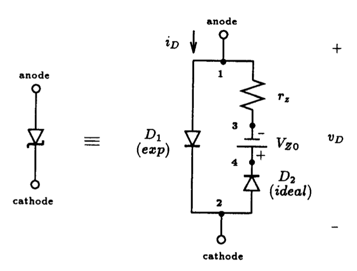
Although the start of the diode breakdown region defined by VZK and IZK can be specified on a diode model statement using the Spice parameters BV and IBV, no control is provided for the user to specify the characteristics of the breakdown region, i.e., slope of the i-v curve in the breakdown region. It is common for zener diode manufacturers to specify the shape of the breakdown region by specifying the inverse of the slope of the almost-linear i-v curve at some operating point (VZ, IZ) inside the breakdown region. This inverse-slope parameter has dimensions of resistance and is known as the dynamic resistance of the zener, denoted as rz.
To model a zener diode the equivalent circuit shown in Fig. 3.13 is sometimes used. When vD > -VZ0, ideal diode D2 is consider cut-off and the terminal characteristics of the zener diode are determined solely by diode D1. Conversely, when vD > -VZ0, ideal diode D2 turns on, whereby a voltage of vD + VZ0 appears across resistor rz. The resulting current that flows through this resistance will be much greater than the reverse-bias leakage current that flows through diode D1, and therefore, the current that dominates the breakdown region of the zener diode is given by the following equation,
(3.7)

The value of VZ0 is not specified directly by the zener diode manufacturer but can be derived from the operating point information at which the dynamic resistance is obtained. It is found from the expression
(3.8)
![]()
The following example will illustrate a common application of a zener diode.
|
Fig. 3.13: A circuit model of a Zener diode. |
Fig. 3.14: A simple voltage regulator circuit with load using a single zener diode.
|

|
Fig. 3.15: Circuit setup used to investigate the line and load regulation of the simple zener diode voltage regulator circuit of Fig. 3.14. |
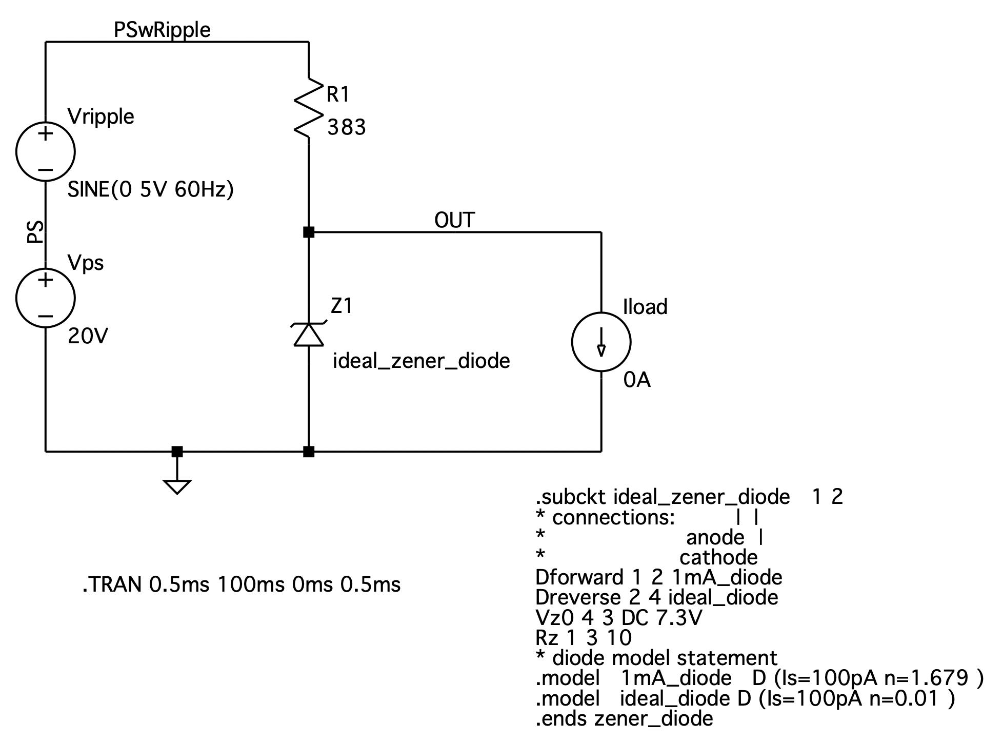
Zener Diode Voltage Regulator Circuit (No Load)
* zener diode subcircuit .subckt ideal_zener_diode 1 2 * connections: | | * anode | * cathode Dforward 1 2 1mA_diode Dreverse 2 4 ideal_diode Vz0 4 3 DC 7.3V Rz 1 3 10 * diode model statement .model 1mA_diode D (Is=100pA n=1.679 ) .model ideal_diode D (Is=100pA n=0.01 ) .ends zener_diode
** Main Circuit ** * power supply Vps PS 0 20V Vripple PSwRipple PS SINE(0 5V 60Hz) * zener diode voltage regulator circuit R1 PSwRipple OUT 383 XZ1 0 OUT ideal_zener_diode * simulated load condition Iload OUT 0 0A ** Analysis Requests ** .TRAN 0.5ms 100ms 0ms 0.5ms .backanno .end
Fig. 3.16: The LTSpice circuit netlist for computing the time-varying no-load output voltage of the zener diode voltage regulator circuit shown in Fig. 3.15.
|
Voltage Regulation using a Zener Diode
Rather than using a string of diodes to create a simple voltage regulator circuit, a single zener diode can be used in its place, as shown in Fig. 3.14. In this example, the regulator circuit was designed for an output voltage of approximately 7.5 V, assuming that the raw supply voltage fluctuates between 15 and 25 V and that the load current can vary between 0 and 15 mA. The zener diode available has a voltage drop of VZ=7.5 V at a current of 20 mA, and its rz equals 10 Ω. The current limiting resistor R in series with the zener diode was chosen at 383 Ω so that the minimum current through the diode never drops below 5 mA. Based on this design, both the line and load regulation were found to be 25.4 mV/V and -9.7 mV/mA, respectively. Using LTSpice, together with the model described above for the zener diode, we would like to confirm that the design requirements are indeed met. Further, we would like to check the line and load regulation directly from simulation results.
To carry out this investigation, we use the circuit setup shown in Fig. 3.15. Here the raw power supply level is modeled with two sources: a DC voltage source VS to model the average value of the power supply level, and a time-varying voltage source vripple to model the fluctuations of the power supply. Specifically, the level of the DC source is set at 20 V, and the fluctuations are modeled as a sinusoidal signal having a peak amplitude of 5 V. The frequency of this source is arbitrarily selected to be 60 Hz. To mimic possible load current fluctuations, a single current source is connected across the output terminals of the voltage regulator. We shall begin our first simulation with the value of this current source set to zero in order to first determine the behavior of the regulator under no-load conditions.
The model for the zener diode is the equivalent circuit shown in Fig. 3.13. The value of rz is simply that specified in the problem at 10 Ω. The value of VZ0 is determined from Eqn. (3.8) and the data supplied for the zener diode (given above), from which we find VZ0= 7.3 V. Diode D1 will be modeled as a 1 mA diode with an emission coefficient of 1.679. The ideal diode, D2, will be model with IS=100 pA and n=0.01. The subcircuit describing this particular zener diode would be as follows:
|
.subckt ideal_zener_diode 1 2 * connections: | | * anode | * cathode Dforward 1 2 1mA_diode Dreverse 2 4 ideal_diode Vz0 4 3 DC 7.3V Rz 1 3 10 * diode model statement .model 1mA_diode D (Is=100pA n=1.679 ) .model ideal_diode D (Is=100pA n=0.01 ) .ends zener_diode
|
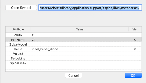
This subcircuit has been copied and placed on the schematic in the command window through the Spice directive utility. In order to use this subcircuit representation, a diode was extracted from the built-in component list, placed on the schematic, then its attributes were edited. To access the attribute table, click the right mouse button while holding down the control-key and the attribute table will appear. Two items in this list need to be changed. The first is the item on the top line line called Prefix. Change the letter D to X, to specific that it is a subcircuit rather than a diode. Next, in the fourth line down from the top, called Value, change this to the title of the subcircuit; in our case here, we are using ideal_zener_diode. To make the symbol more relevant to what we are doing here, the instname was changed from D1 to Z1. On completion, one would see the following :
Remember that the Zener diode is used in its reverse breakdown region not the forward bias region as a regular signal diode. In addition, a transient analysis is requested so that 6 periods of the output voltage signal can be observed. The resulting schematic as captured by LTSpice is shown in Fig. 3.15, along with the circuit netlist shown in Fig. 3.16.
|
|
|
Fig. 3.17: Several waveforms associated with the zener-diode-regulator circuit of Fig. 3.14 under no-load conditions. The top graph displays the voltage generated by the power supply and the bottom graph displays the corresponding output voltage from the regulator circuit.
|
The results of the Spice analysis are shown in Fig. 3.17. Both the power supply voltage VS + vripple and the voltage across the zener diode are shown. The top graph displays the supply voltage and the bottom graph displays the corresponding zener diode voltage waveform. As expected, the voltage fluctuation of the power supply is sinusoidal having a peak-to-peak amplitude of 10 V riding on a DC level of 20 V. The output voltage from the regulator circuit is also sinusoidal having a peak-to-peak amplitude of 254.7 mV and riding on a DC level of 7.628 V. The precise value of these two levels were determined using the cursor facility of the waveform viewer. One can also notice that both the input and the output voltage waveforms are in phase. Thus, we can conclude that a line voltage change of +10 V gives rise to an output voltage change of +254.7 mV. Thus, the line regulation, given by
is calculated to be +25.47 mV/V. This seems to agree almost exactly with the value determine by the simple expression for line regulation given by rz/(rz+R) (i.e., 25.4 mV/V). This should not be too surprising here given that the circuit has been operating entirely in its linear region.
|
Fig. 3.18: The output voltage of the zener diode regulator circuit of Fig. 3.14 when the load current varies between 0 and 15 mA. The top graph displays the current drawn by the load, and the bottom graph displays the corresponding output voltage from the regulator circuit.
|
Fig. 3.19: Observing a worst-case situation: The top-most graph displays the minimum power supply voltage, the middle graph displays the time-varying load current, and the bottom graph displays the current flowing through the zener diode.
|


We can perform a similar analysis to that above, but this time, with the load current varying between 0 and 15 mA. In this way we can determine the load regulation by observing the output voltage waveform. The power supply voltage will be assumed constant at +20 V. We shall assume that the load current is triangular with a minimum value of 0 mA and a maximum value of 15 mA. The frequency of this signal will be made arbitrarily equal to 30 Hz, corresponding to a period of 33.33 ms. This signal will correctly model the minimum and maximum fluctuations of the load current. Consider revising the statement for the output current source iLoad seen in the LTSpice command window of Fig. 3.15 according to the following:
Iload 2 5 PULSE (0mA 15mA 0 16.66ms 16.66ms 0 33.33ms 3).
Here a triangular waveform is emulated using the source PULSE statement. The rise time and fall time are set equal to one-half the period of the triangular waveform of 33.33 ms and the Ton or pulse-width is set to 0 s.
The amplitude of the ripple voltage superimposed on the DC supply voltage should be set to 0 V in order to eliminate its presence during this analysis. Therefore, the attributes for this source are changed to the following:
Vripple PSwRipple PS SINE(0 0V 60Hz)
On execution, the output voltage waveform VO for the regulator circuit is shown in the bottom graph of Fig. 3.18. The waveform shown in the top graph depicts the load current iLoad. Here the load current is triangular, as it should be, with a 15-mA peak-to-peak amplitude. The corresponding output voltage signal is also triangular of the same frequency. The peak-to-peak amplitude of this signal was found using the cursor facility of the waveform viewer to be 146.33 mV. For an average load current of 7.5 mA, the output voltage corresponds to 7.555 V. It is important to notice that the phase of the output voltage waveform is opposite to that of the load current. This suggests that for a change in the load current of +15 mA, the output voltage changes by -146.33 mV, thus suggesting that the load regulation, expressed as

would be -146.33 mV / 15 mA, or -9.7 mV/mA. This agrees exactly with the value determine by the simple expression for load regulation given by -rz||R.
As a final check on this design, let us investigate the minimum current that flows through the zener diode. Observe that the zener diode current is minimum when the power supply voltage is at its minimum and the load current is at its maximum. In keeping with our earlier approach, we shall maintain the load current as a triangular wave varying linearly between 0 and 15 mA. The ripple voltage vripple simulating fluctuations in the power supply voltage will be set to a constant -5 V level. This requires that the LTSpice statement for this source be changed to a DC source of -5 V according to following:
Vripple PSwRipple PS -5V
Re-running the LTSpice analysis with the revised source statement results in the three waveforms shown in Fig. 3.19. The top graph displays the constant +15 V level associated with the power supply and the graph below it displays the load current waveform. The lowest-most graph displays the current waveform associated with the zener diode. As is evident, the current through this diode varies between -5 mA and -20 mA. For all practical purposes, based on the LTSpice results above, we can conclude that all aspects of the design did indeed meet the required conditions.
|
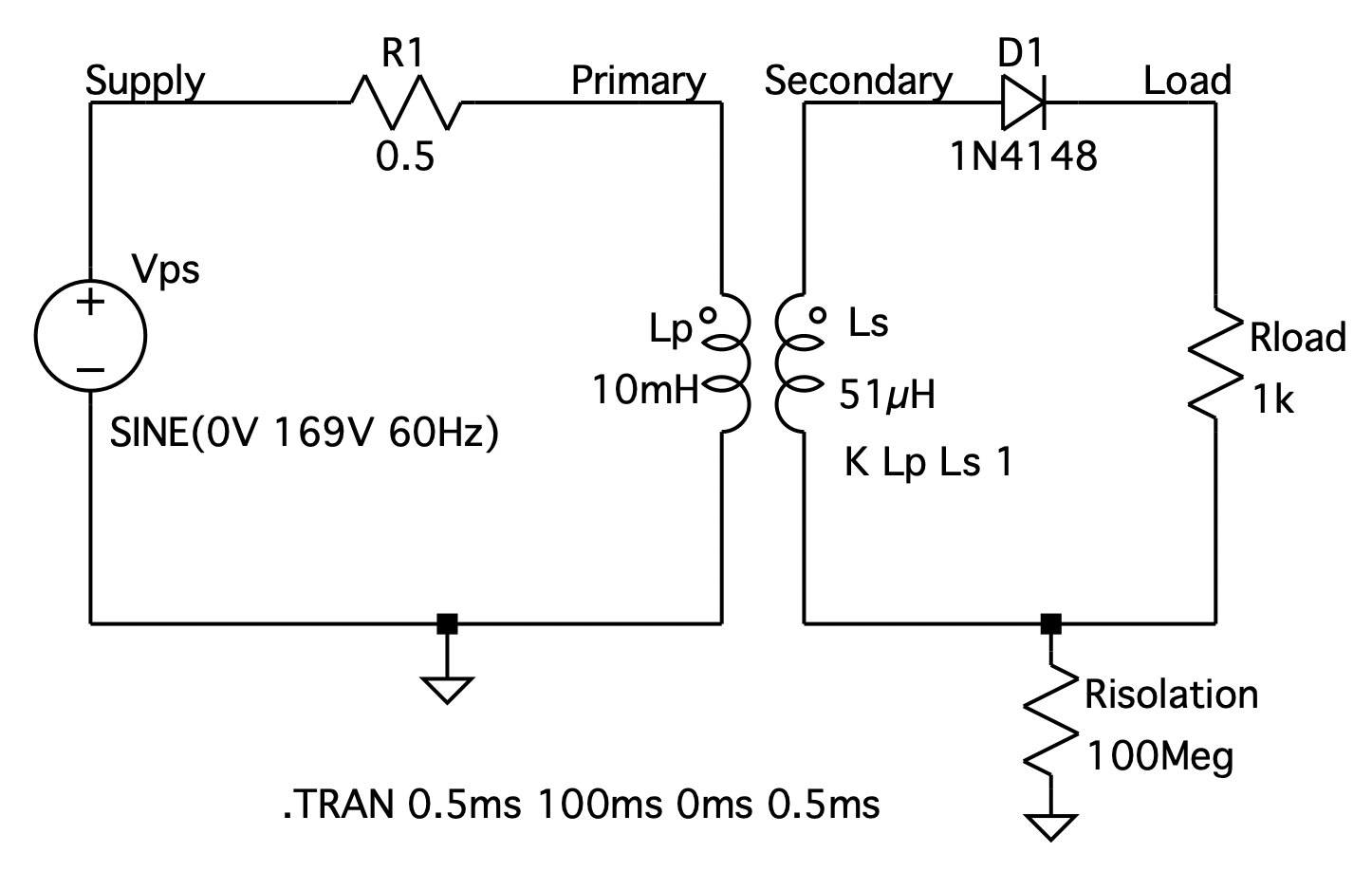
Fig. 3.20: Half-wave rectifier circuit using a transformer with a 14:1 turns ratio to step down the line voltage of 120 V-rms to 12 V-peak.
|
Fig. 3.21: The general syntax of the Spice statements used to describe a (nonideal) transformer. The transformer turns ratio NP:NS is determined by the appropriate selection of primary and secondary inductor values, LP and LS, respectively.
|


|
Fig. 3.22: Preparing the half-wave rectifier circuit shown in Fig. 3.20 for LTSpice analysis: A large-valued isolation resistor (100 MW) is placed between the secondary side of the transformer and ground. This provides a DC path between the secondary side of the transformer and the common reference node (0).
|
Half-Wave Rectifier Circuit * * Circuit Description * * ac line voltage Vps Supply 0 SINE(0V 169V 60Hz) R1 Primary Supply 0.5 * transformer section Lp 0 Primary 10mH Ls N001 Secondary 51µH K Lp Ls 1 * isolation resistor (allows secondary side to pseudo-float) Risolation N001 0 100Meg * diode current monitor VD1 2 6 0 * rectifier circuit D1 Secondary Load 1N4148 Rload Load N001 1k * diode model statement .lib /Users/roberts/Library/Application Support/LTspice/lib/cmp/standard.dio * unused diode statements .model D D * * Analysis Requests * .TRAN 0.5ms 100ms 0ms 0.5ms .backanno .end
Fig. 3.23: The LTSpice circuit netlist for calculating the transient behavior of the half-wave rectifier circuit corresponding to the circuit in Fig. 3.22.
|
3.4 Rectifier Circuits
One of the most important applications of semiconductor diodes is in the design of rectifier circuits. In the following, with the aid of LTSpice, we shall investigate two common types of rectifier circuits: the half-wave and the full-wave rectifier. In the case of the full-wave rectifier, we shall consider it in conjunction with a peak rectifier circuit. Subsequently, we shall combine this full-wave rectifier circuit with a zener diode voltage regulator circuit to form a complete power supply circuit.
3.4.1 Half-Wave Rectifier
A half-wave rectifier circuit is shown in Fig. 3.20. It consists of a transformer with a 14:1 turns ratio, a single diode D1 of the commercial type 1N4148, and a load resistance Rload of 1 kΩ. The source resistance of 0.5 Ω of the AC line is also included in this circuit. The purpose of the transformer is to step down the main household AC power supply voltage of 120 V-rms to a 12 V-peak level. Spice does not make provision for an ideal transformer, probably for a good reason; one does not exist in practice. Instead, Spice allows coupled inductors to be described having a coefficient of coupling k between 0 and unity. Two inductors, say for example, LP and LS, which share a common magnetic path and have a coefficient of coupling, k. The turns ratio NP/NS of such a transformer is given by the square-root of the ratio of the primary to secondary inductance, i.e., NP/NS = ÖLP/ÖLS.
To describe such a transformer to LTSpice, two inductors are placed on the schematic in the LTSpice command window. The magnetic phasing of each inductor must be made visible to ensure one connects the inductors according to the ``dot’’ convention. This is done by placing the mouse cursor over the inductor and clicking the right button of the mouse and setting the “Show Phasing Dot” box. A component can be rotated using control-R or mirrored using control-E commands to ensure the appropriate phase arrangements are made. Finally, in a rather unorthodox manner, the coefficient of coupling, k, is set through a Spice directive command using the following syntax:
Kname Lp Ls k-value
No ``dot’’ precedes this statement as any other Spice directive and, further, the Spice Directive box must be selected. In other words, don’t make it a Comment statement. A summary of this can be found in Fig. 3.21. Extension to three or more coupled inductors follows a similar format. This will be introduced in the next example.
Returning to the half-wave rectifier circuit of Fig. 3.20, we can create a LTSpice description of this circuit. We shall assume that the inductance of the primary side of the transformer is 10 mH, and the inductance of secondary side is 51 𝜇H. This will provide an effective transformer turns ratio of 14:1. Continuing, the alert student will quickly realize that the circuit on the secondary side of the transformer has no DC path to ground and will therefore report false information. To circumvent this situation, we simply add a large resistor between ground and one point on the secondary side. The value of this resistor should be chosen such that it does not significantly interfere with the operation of the circuit. A 100 Meg-Ω resistor was chosen to be placed between the load and ground. The 1N4148 type diode is selected from the library of commercial diodes made available in LTSpice. After placing the diode on the schematic of the command window, place the cursor of the mouse over the diode and right click. The diode attribute window appears. Click the button highlighted with ``Pick New Diode’’ and scroll down the list that appears for the 1N4148 diode model. A transient analysis is requested to compute the voltage appearing across the load resistance, the voltage appearing across the primary- and secondary-side of the transformer, and finally, the AC line voltage for six cycles. To identify these signals clearly, each of these nodes have been labeled. The resulting schematic is shown in Fig. 3.22 and the corresponding circuit netlist is seen listed in Fig. 3.23.
|
Fig. 3.24: Various voltage waveforms associated with the half-wave rectifier circuit shown in Fig. 3.22. The top graph displays both the AC line voltage and the voltage appearing across the primary side of the transformer. The bottom graph displays the voltage appearing across the load resistor and the voltage appearing across the secondary side of the transformer.
|
Fig. 3.25: Zooming-in on a half cycle of the voltage waveform appearing across the load resistor and comparing it to the voltage developed across the secondary-side of the transformer.
|

|
|
|
Fig. 3.26: The voltage and current waveform associated with diode D1. The peak inverse voltage (PIV) is seen to be 12 V and the maximum diode current is 11.1 mA. |

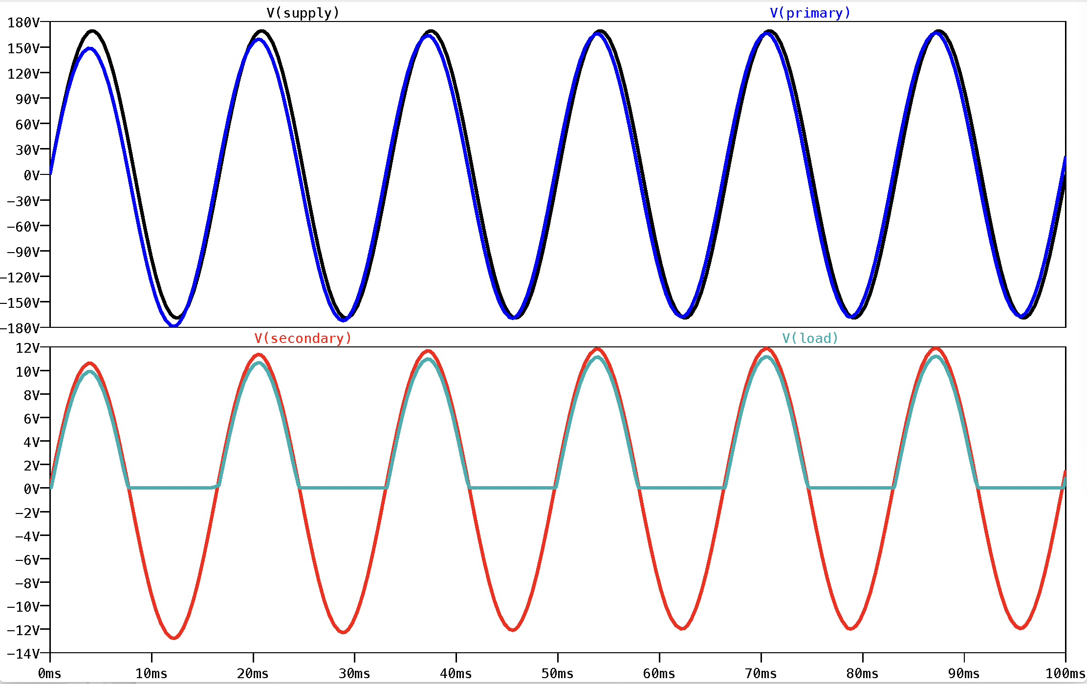
The results of the transient analysis are shown in Fig. 3.24. The top graph displays the voltage waveform of the AC line voltage (Vac) and the voltage appearing across the primary side of the transformer. Here we see that the voltage across the transformer experiences a short transient effect, quickly settling into its steady state with the transformer voltage slightly lagging behind the line voltage. The bottom graph displays the rectified voltage appearing across the load resistance and the voltage appearing across the secondary side of the transformer. A blown-up view of a half period of the rectified output voltage and the transformer secondary-side voltage is shown in Fig. 3.25.
An important consideration in the design of rectifier circuits is the diode current-handling capability, determined by the largest current that it has to conduct, and the peak inverse voltage (PIV) that the diode must be able to withstand without breakdown. In Fig. 3.26 we display both the voltage across the diode and the current that it conducts. We see that the PIV of this particular rectifier circuit is 12 V. Because the diode has not broken down, we can assume that the breakdown voltage of the 1N4148 commercial diode is larger than 12 V. In fact, data sheets of the 1N4148 diode indicate that its breakdown voltage is in the vicinity of 100 V. The maximum current that the diode has to conduct is seen to be about 11 mA. Using the cursor facility of the waveform viewer, we find that it is 11.1 mA. The data sheets of the 1N4148 indicate that this diode can handle a peak current of no more than 100 mA, thus our rectifier design is well within the limits of the 1N4148.
|
(a)
(b)
Fig. 3.27: (a) A full-wave peak rectifier circuit. (b) Actual circuit set-up for LTSpice.
|
Full-Wave Peak Rectifier Circuit
* * Circuit Description * * ac line voltage Vps Supply 0 SINE(0V 169V 60Hz) R1 Primary Supply 0.5 * transformer section with center-tap Lp 0 Primary 10mH Ls1 Load- Secondary 51µH Ls2 N001 Load- 51µH K Lp Ls1 Ls2 0.9 * isolation resistor Risolation Load- 0 100Meg * full-wave peak rectifier circuit D1 Secondary Load+ 1N4148 D2 N001 Load+ 1N4148 Rload Load+ Load- 1k Cload Load+ Load- 50µF * diode model statement .lib /Users/roberts/Library/Application Support/LTspice/lib/cmp/standard.dio * unused diode statements .model D D * * Analysis Requests * .TRAN 0.1ms 100ms 0ms 0.1ms .backanno .end
Fig. 3.28: The Spice input file for calculating the transient response of a full-wave peak rectifier circuit. |


3.4.2 Full-Wave Peak Rectifier
Fig. 3.27(a) displays a circuit for a full-wave peak rectifier. It consists of a full-wave rectifier - diodes D1 and D2 and a center-tapped transformer - and a filter capacitor C to smooth the voltage that appears across the load resistor R. Also shown is the resistance of the input voltage source of 0.5 Ω. The transformer is center tapped with each coil on the secondary side having a turns ratio of 14:1 with respect to the primary coil. In Fig. 3.27(b) we display the circuit that we shall actually describe to LTSpice for analysis. An isolation resistance RIsolation has been added to the circuit on the secondary side of the transformer in order to provide a DC path to ground.
In the following we shall analyze the rectifier circuit of Fig. 3.27 with LTSpice assuming that the peak rectifier has a load resistance of 1 kW and a smoothing capacitor of 50 𝜇F. The two rectifier diodes will be assumed to be modeled after the commercial 1N4148. To obtain a transformer with a primary-to-secondary turns ratio of 14:1 for each coil on the secondary side, we have assumed that each coil of the secondary side has an inductance of 51 𝜇H. This, then, implies that the inductance of the primary must be 10 mH according to the relationship: NP/NS = ÖLP/ÖLS. Further, we have also assumed a coefficient of coupling between each coil at a value of 0.9. The center-tapped transformer is described by the following three inductor statements with a corresponding a coefficient of coupling:
|
* transformer section with center-tap Lp 0 Primary 10mH Ls1 Load- Secondary 51µH Ls2 N001 Load- 51µH K Lp Ls1 Ls2 0.9
|
The LTSpice netlist describing this circuit can be seen in Fig. 3.28. It includes a transient analysis that is performed over six periods of input line voltage. As our first analysis, the voltage waveform that appears across the load resistor and the voltage waveform that appears across one coil on the secondary side of the transformer is shown in Fig. 3.29. As is evident, the voltage appearing across the load resistor initially ramps up from 0 V to a steady-state value that ripples somewhere between 9 and 10 V. Using the cursor facility of the waveform viewer, we are able to determine more precisely the minimum and maximum values of this output voltage waveform to be 8.8 and 10.1 V, respectively. Thus, the average voltage appearing across the load resistor is 9.42 V having a peak-to-peak ripple voltage of 1.25 V. Also shown in the graph of Fig. 3.29 is the voltage waveform appearing across the secondary-side coil LS1 of the transformer (see Fig. 3.27). Here we see that it settles into a sinusoidal with a peak value of 10.8 V. It is not quite at the ideal peak level of 12 V, as the coefficient of coupling is somewhat less than unity (i.e., k=0.9)
|
|
|
Fig. 3.29: Voltage waveforms associated with the peak-rectifier circuit shown in Fig. 3.27. One waveform is the voltage that appears across the load resistance R and the other waveform is the voltage that appears across LS1 on the secondary side of the transformer.
|

Next, let us consider investigating the current that flows through each diode of the rectifier. According to a hand analysis, together with the assumption that the forward voltage drop across each diode is 0.8 V, the expected ripple associated with this circuit using the equation Vr = VP/(2 f C R) is 1.86 V. This appears to be slightly larger than that observed from the above simulations. As we shall soon discover, the reason for the discrepancy is largely due to the large series resistance rS of 16 Ω associated with each diode. It is interesting to point out that the average load voltage (VL= VP - Vr/2) agrees quite closely with the value obtained from the above simulation at 10.26 V.
|
Fig. 3.30: The instantaneous current flowing through each diode of the rectifier.
|
Fig. 3.31: A close-up view of a single current pulse in steady state flowing through diode D2. |


To further investigate the behavior of the full-wave peak rectifier circuit shown in Fig. 3.27, the waveforms of the current that flows through each diode is plotted in Fig. 3.30. The top graph displays the current that flows through diode D1 and the graph below it displays the current waveform associated with diode D2. As is evident from the top graph, diode D1 conducts a rather large initial current pulse having a peak value of about 200 mA and seems to have reached steady-state behavior by the fourth current pulse. The current waveform associated with diode D2 does not reveal such a dramatic transient, instead it appears to have reached steady state by the third current pulse.
To see more closely a single steady-state pulse of the current that flows through diode D2, we expanded the horizontal scale of the bottom graph shown in Fig. 3.30 between 90 and 100 ms and plotted an expanded view of the current waveform shown there in Fig. 3.31. Here we find that the current pulse has a peak value of about 91 mA and extends between 94.0 ms and 96.0 ms for a conduction period of 2.0 ms. According to the simple theory developed for full-wave rectifier circuits, the expected conduction period Dt of each diode is given by
(3.9)
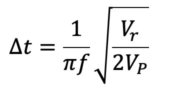
and the peak diode current iD,MAX (in steady-state) is given by
(3.10)
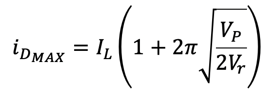
Substituting the appropriate numerical values, we estimate the conduction period of either diode in steady state to be 1.53 ms. Similarly, the peak diode current is expected to be 122.1 mA. Comparing these two results with those found through simulation (2.0 ms and 91 mA), we find that they differ significantly. On investigation we discovered that the major reason for the discrepancies between theory and the LTSpice simulation is the presence of the nonzero bulk diode resistance rS. In the mathematical development of the formulae that describe the full-wave rectifier circuit, the series resistance associated with a practical diode was not accounted for (mainly to keep the mathematical description simple).
|
(a)
(b)
Fig. 3.32: A 5 V regulated power supply: (a) circuit schematic, and (b) circuit schematic captured by LTSpice with zener diode subcircuit model.
|
A Regulated Power Supply * * zener diode subcircuit * .subckt 5.1V_zener_diode 1 2 * connections: | | * anode | * cathode Dforward 1 2 1mA_diode Dreverse 2 4 ideal_diode Vz0 4 3 DC 4.9V Rz 1 3 10 * diode model statement .model 1mA_diode D (Is=100pA n=1.679 ) .model ideal_diode D (Is=100pA n=0.01 ) .ends zener_diode
* * Main Circuit * * ac line voltage Vps Supply 0 SINE(0V 169V 60Hz) R1 Primary Supply 0.5 * transformer section with center-tap Lp 0 Primary 10mH Ls1 Load- Secondary 51µH Ls2 N002 Load- 51µH K Lp Ls1 Ls2 0.9 * isolation resistor Risolation Load- 0 100Meg * full-wave peak rectifier circuit D1 Secondary N001 1N4148 D2 N002 N001 1N4148 Cload N001 Load- 583µF R2 N001 Load+ 160 * zener diode XZ1 Load- Load+ 5.1V_zener_diode * load Rload Load+ Load- 500 * diode model statement .lib /Users/roberts/Library/Application Support/LTspice/lib/cmp/standard.dio * unused diode statements .model D D * * Analysis Requests * .TRAN 0.1ms 100ms 0ms 0.1ms .backanno .end
Fig. 3.33: The LTSpice-generated circuit netlist for calculating the time-varying output voltage of the 5 V regulated power supply shown in Fig. 3.32.
|

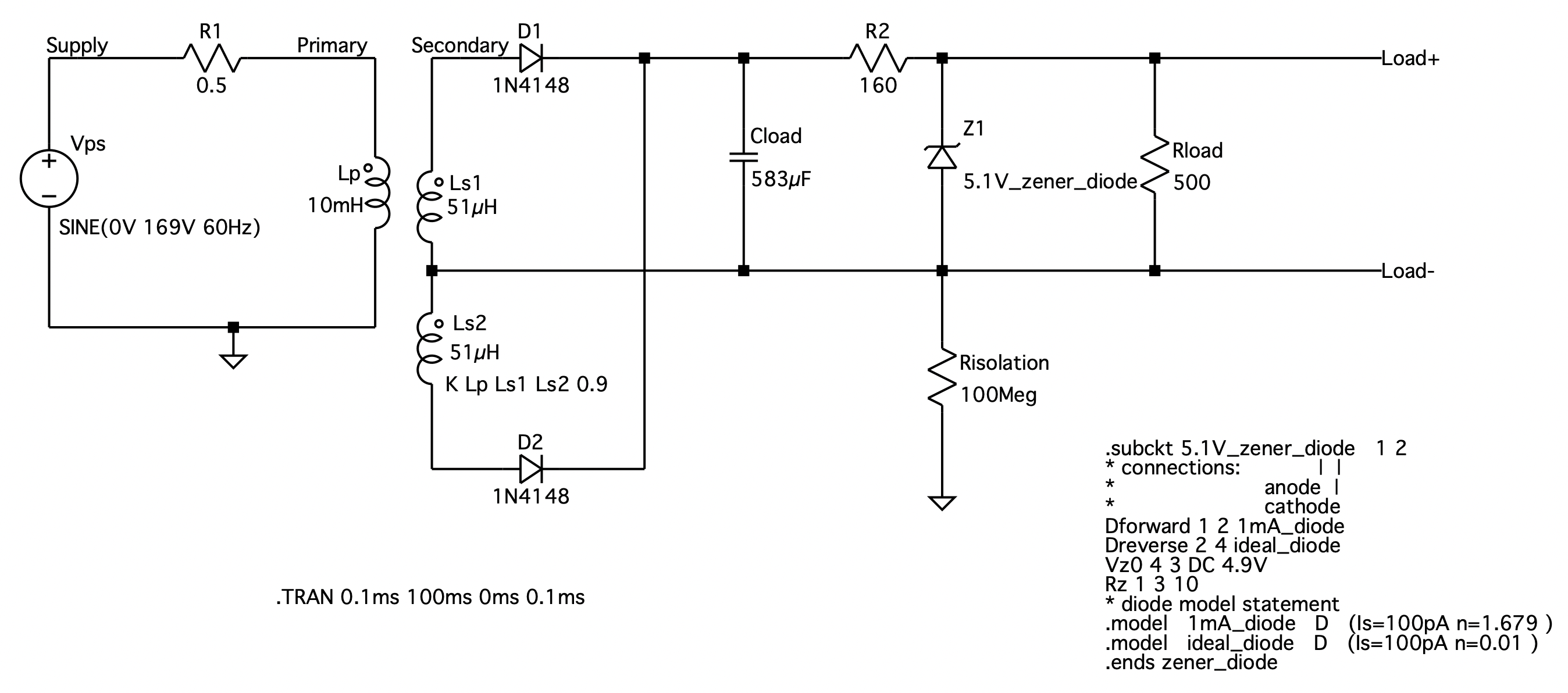
3.4.3 A Voltage Regulated Power Supply
To complete this section on rectifier circuits we shall analyze a commonly used power supply configuration with LTSpice. Consider the circuit shown in Fig. 3.32. It can be thought of as consisting of three parts: a full-wave peak rectifier, a Zener-diode-voltage regulator and the load. The peak rectifier circuit acts to supply a relatively stable DC voltage to the zener regulator which, in turn, reduces any voltage fluctuation (ripple) that appears on it. In addition, the voltage regulator acts to maintain a constant voltage across the load for a wide range of load currents. Resistor RIsolation is used for LTSpice simulation purposes and plays no role in the circuit function.
Let us consider using the circuit configuration shown in Fig. 3.33 to design a 5 V power supply for an application that requires a maximum load current of 20 mA. The 120 V-rms AC household voltage is stepped down to a 12 V-peak level using a center-tapped transformer with each coil on the secondary side having a turns ratio of 14:1 with respect to the primary coil. Further, we have at our disposal a zener diode that has VZ=5.1 V at a current of 20 mA and has a dynamic resistance rz=10 W. We also know that the minimum zener diode current must be limited to 5 mA if we are to maintain the diode in its breakdown region. Assuming that the input voltage to the voltage regulator circuit ranges between 9 and 12 V, we choose the current limiting resistor R from the expression:
(3.11)
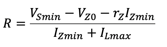
Thus, we obtain R=160 W. As a point of reference, under worst-case conditions, the expected minimum output voltage is about 4.95 V as calculated from the expression, VOmin = VZ0 + rz IZmin.
The size of the smoothing capacitor is to be determined so that the voltage applied to the regulator circuit does not go below 9 V. Assuming that the peak voltage appearing across the secondary-side of the center-tapped transformer is 12 V, then the worst-case ripple voltage must be limited to no more than 3 V. We shall limit the ripple voltage to a more conservative 1 V level in case the peak voltage level changes. We can then estimate the size of the capacitor we require by using the formula for the ripple voltage for a full-wave peak rectifier, i.e.,
(3.12)
![]()
Substituting R=160 Ω, Vr=1 V, VP=11.2 V (accounting for a 0.8 V diode drop) and f=60 Hz, we get C=583 𝜇F. This capacitance may seem large but is typical of the size of capacitor used in power supplies.
To investigate whether our design meets the required specifications, we shall simulate the power supply circuit shown in Fig. 3.32(a) with an initial load resistance of 500 W. This load should draw an average current of no more than 10 mA - well within the maximum load current condition. The schematic captured by LTSpice is seen in Fig. 3.32(b). The transformer is represented by a primary inductance of 10 mH, and the two coils on the secondary side are each assigned a value of 51 uH. The coefficient of coupling for the three inductors is set to 0.9. The two rectifier diodes are assumed to be modeled after the commercial diode type 1N4148. The circuit netlist generated by LTSpice is shown listed in Fig. 3.33.
The first analysis that we shall perform with LTSpice is to determine whether the output voltage is nominally 5 V. This can be determined by observing the voltage across the load resistance. Due to the presence of the large smoothing capacitor C, a long charge-up time will be necessary before the power supply circuit reaches steady-state. Therefore, a request for a long transient analysis is necessary to observe steady-state behavior. Here we have selected that the transient be computed over a 100 ms interval. On completion of the LTSpice analysis, the voltage waveform that appears across the 500-Ω load resistor is shown in Fig. 3.34. Also shown is the voltage that appears across the smoothing capacitor C. As we can see, the voltage across the capacitor has an average value of about 10.5 V and a peak-to-peak ripple of 0.5 V. In contrast, the voltage across the load resistor is quite close to 5 V. Using the cursor facility of the waveform viewer, we find that the load voltage ripples slightly, between 5.13 and 5.17 V, a ripple voltage of only 36 mV. We therefore see that the above power-supply design is operating quite close to the nominal design, providing an output voltage of 5 V at a load current of about 10 mA.
|
Fig. 3.34: The voltage across the smoothing capacitor C of the peak rectifier, and the output voltage across the 500 W load resistance.
|
Fig. 3.35: The output voltage waveform from the 5 V power supply for load resistances of 50, 100, 150, 200, 250 and 500 W. The voltage regulation is lost at a load resistance below 150 W.
|


To see the effect of larger current demands on the power supply, consider reducing the load resistance. In order to compare the effect of different loads, we shall re-simulate the circuit with load resistances of: 50, 100, 150, 200 and 250 Ω. Assuming that these load resistances do not significantly affect the output voltage, they would correspond to a load current of: 33.3 mA, 25 mA and 20 mA, respectively. Using the previous LTSpice command window, the following .STEP directive was included to enable the three different loads
.STEP param Rload LIST 50 100 150 200 250 500
and the load resistor of 500 Ω was re-assigned a variable denoted as {Rload}. As a result of the transient analysis, we display a view of the output voltage over the time interval 50 to 100 ms in Fig. 3.35. As is clearly evident, for load resistances greater than and including 150 Ω, the output voltage is maintained very near the 5 V level with very little ripple visible. However, for a load resistance less than 150 Ω, we see that the output voltage level has dropped down to an average value of about 4.15 V. Also, we see that the ripple voltage associated with this signal has increased significantly. This suggests that the output voltage is no longer being regulated. This is because the zener diode has been starved of its current and has turned off.
We conclude that the power supply circuit shown in Fig. 3.32 will provide a constant 5 V output level for load currents at least as large as 33 mA.
3.5 Limiting and Clamping Circuits
In the following we shall simulate the circuit operation of several commonly used diode circuits. This will include the analysis of a back-to-back diode limiter circuit, a DC restorer circuit and a voltage doubler circuit.
|
(a)
(b)
Fig. 3.36: A back-to-back diode limiter circuit: (a) circuit schematic, and (b) circuit schematic captured by LTSpice using commercially available diode 1N4148.
|
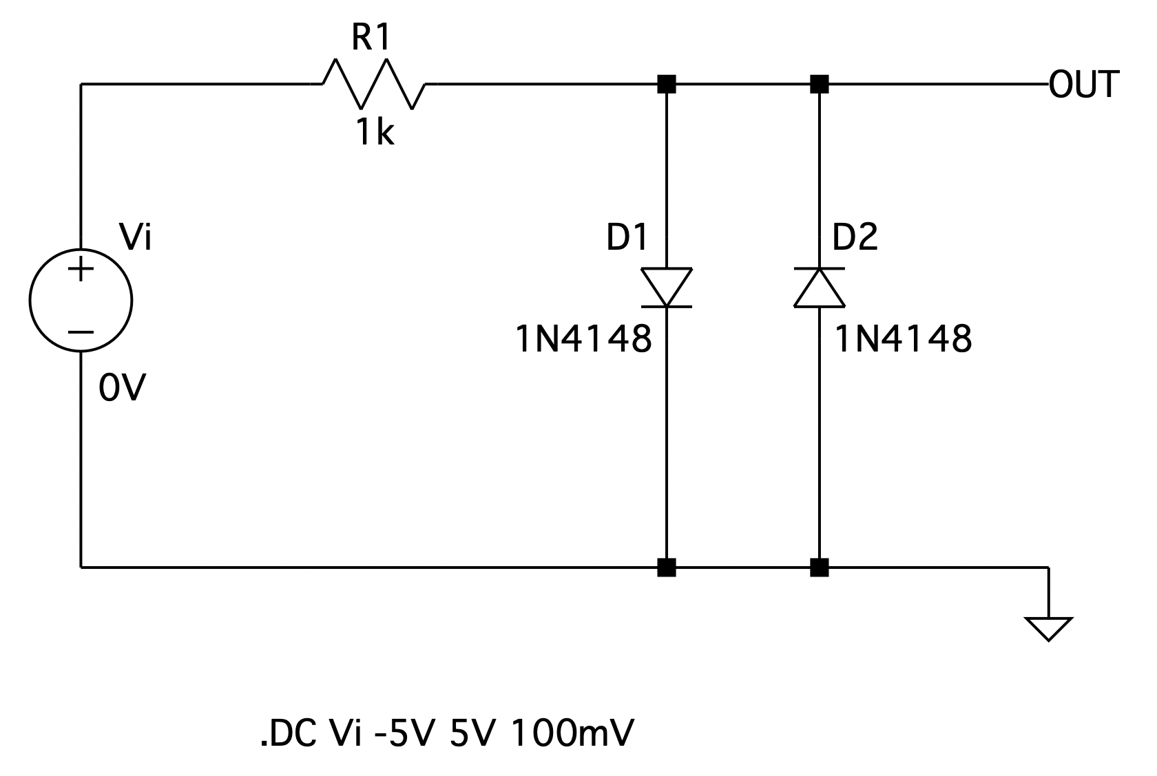
A Diode Limiter Circuit
* * Circuit Description * Vi N001 0 0V R1 OUT N001 1k D1 OUT 0 1N4148 D2 0 OUT 1N4148 * diode model statement .lib /Users/roberts/Library/Application Support/LTspice/lib/cmp/standard.dio * unused diode statements .model D D * * Analysis Requests * * sweep the input voltage level from -5 V to +5 V in 100 mV increments .DC Vi -5V 5V 100mV .backanno .end
Fig. 3.37: The LTSpice generated circuit netlist for calculating the DC transfer characteristic of the back-to-back diode limiter circuit of Fig. 3.36.
|

|
|
Fig. 3.38: DC transfer characteristic of the back-to-back diode limiter shown in Fig. 3.36. |

A Diode Limiter Circuit
In Fig. 3.36(a) we present a simple back-to-back diode limiter circuit constructed with two diodes of the 1N4148 type. Using LTSpice, we would like to observe the transfer characteristic of such a circuit. The circuit schematic captured by LTSpice is shown in Fig. 3.36(b) and the corresponding circuit netlist is listed in Fig. 3.37. Here the input DC source Vi is swept between -1 and +1 V. On execution, the transfer characteristic is shown in Fig. 3.38. Here we see that the transfer characteristic exhibits rather soft limiting with the linear region ranging between -0.5 V and +0.5 V. The slope in the linear region is found to be unity.
|
(a)
(b)
Fig. 3.39: A DC restorer circuit: (a) circuit schematic, and (b) circuit schematic captured by LTSpice using commercially available diode 1N4148. |
A DC Restorer Circuit * * Circuit Description * Vi IN 0 PULSE(-3 7 0s 10us 10us 0.490ms 1ms) C1 OUT IN 1µ D1 0 OUT 1N4148 * diode model statement .lib /Users/roberts/Library/Application Support/LTspice/lib/cmp/standard.dio * unused diode statements .model D D * * Analysis Request * .TRAN 100u 10m 0m 100u .backanno .end
Fig. 3.40: The LTSpice generated circuit netlist for calculating the time-varying output voltage from the DC restorer circuit shown in Fig. 3.39.
|


|
|
|
Fig. 3.41: The input and output voltage waveforms of the associated with the DC restorer circuit of Fig. 3.39.
|

A DC Restorer Circuit
In Fig. 3.39 we present a DC restorer or a clamped capacitor circuit. Using LTSpice, we would like to observe the transient behavior of this circuit with a square-wave input having a 10 V peak-to-peak amplitude, a +2 V DC offset, and a 1 kHz frequency. The diode will be assumed to be of the 1N4148 type, and the capacitor has a 1 𝜇F value. The LTSpice generated circuit netlist for this particular example is shown in Fig. 3.40. The square-wave input is described by the following source PULSE statement:
Vi 1 0 PULSE ( -3 7 0s 10us 10us 0.490ms 1ms ).
It goes between -3 and 7 V with 0 s delay, a rise and a fall time of 10 us and has a period of 1 ms.
The results of the LTSpice transient analysis are shown in Fig. 3.41. The top graph displays the input 10 V square-wave signal and the bottom graph shows the corresponding signal that appears at the output. We see that it is also a 10 V square-wave, but its DC level has now changed to a 5 V level (one-half the peak-to-peak value).
|
(a)
(b)
Fig. 3.42: A voltage doubler circuit: (a) circuit schematic, and (b) circuit schematic captured by LTSpice using commercially available diode 1N4148.
|
A Voltage Doubler Circuit * * Circuit Description * Vi IN 0 SINE(0 10V 1k) D1 OUT1 0 1N4148 C1 OUT1 IN 1µ D2 OUT2 OUT1 1N4148 C2 0 OUT2 1µ * diode model statement .lib /Users/roberts/Library/Application Support/LTspice/lib/cmp/standard.dio * unused diode statements .model D D * * Analysis Requests * .TRAN 100u 10m 0m 100u .backanno .end
Fig. 3.43: The LTSpice generated circuit netlist for calculating the transient response of the voltage doubler circuit shown in Fig. 3.42.
|


|
|
|
Fig. 3.44: Various voltage waveforms of the voltage doubler circuit shown in Fig. 3.42. The top graph displays the input sine-wave voltage signal, the middle graph displays the voltage across diode D1, and the bottom graph displays voltage that appears at the output.
|

Voltage Doubler Circuit
In Fig. 3.42 we show a voltage doubler circuit. Using LTSpice, we would like to observe the transient behavior of this circuit for an input sine-wave signal having a 10 V amplitude and a 1 kHz frequency. The diodes will be assumed to be of the 1N4148 type, and the two capacitors are of the same value at 1 𝜇F. The LTSpice generated circuit netlist for this particular example is shown in Fig. 3.43.
The results of the transient analysis are shown in Fig. 3.44. Three traces can be seen. The black trace displays the input 10 V-peak sinewave signal, the blue trace displays the voltage signal that appears across diode D1 and the red trace shows the voltage signal that appears at the output of the doubler circuit. Looking closely at the output voltage waveform, we see that it experiences a transient that lasts for about 7 ms and then settles to a constant level of -18.8 V. The magnitude of this signal is approximately twice the peak value of the input sine-wave signal. The voltage across diode D1 settles into a 10 V-peak sine-wave signal with a -10 V DC offset.
3.6 Chapter Summary
· LTSpice can emulate the behavior of a laboratory curve-tracer through the application of the DC sweep command.
· The effect of temperature on a circuit can be investigated using LTSpice.
· An ideal diode can be very well approximated by setting the emission coefficient n of the diode model between 0.01 and 0.001.
· Many commercially available signal, power and zener diodes are represented by a diode model statement found in LTSpice.
· A zener diode can also be represented by a subcircuit description; to simplify its inclusion, use any zener diode found in the LTSpice library, alter its attributes by changing D to X, and link to the subcircuit description.
· An ideal transformer is not represented in LTSpice; instead it is closely approximated by two inductors with a coefficient of mutual coupling, k; a value of k close to unity causes simulations issues.
3.7 LTSpice Tips
· A circuit component can be assigned a parameterized value by identifying its value between brackets { parameter } and including the following Spice directive:
.PARAM parameter = value
· Often one is required to compare the simulation results of one active device with others. To gather the results into one display window, a .STEP directive can be used to cycle through a listing of device models once the model name is given an “ako” (a kind of) designation. For example, assuming the following two models of diode behavior are assigned as follows:
·
|
.model 1mA_diode D (Is=100pA n=1.679) .model 1 ako:1ma_diode
.model bkdwn_diode D (Is=100pA n=1.679 BV=10V IBV=1nA) .model 2 ako:bkdwn_diode |
The following .STEP command can be used to perform two simulations involving these two device models:
.STEP PARAM model_parameter LIST {model_numbers}
· The temperature of a circuit can be changed under some Spice directive using the .TEMP Spice directive command:
.TEMP temperature_list
3.8 Problems
3.1. Assuming that the diodes in the circuits of Fig. P3.1 are modeled with parameters: IS=10-14 and n=2. Determine, with the aid of Spice, values of the labeled voltages and currents. Repeat with diode parameters: IS=10-12 and n=1.
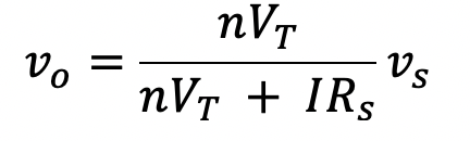
3.2. Consider the battery charger circuit shown in Fig. P3.2. If vS is a 60 Hz sinusoid with 24 V-peak amplitude, find the fraction of each cycle during which the diode conducts. Also find the peak value of the diode current and the maximum reverse-bias voltage that appears across the diode. Assume that the diode has Spice model parameters: IS=10-12 and n=1.6.
3.3. If the sinusoidal source of Problem 3.2 is replaced by a square wave of the same frequency and amplitude, for what fraction of the cycle does the diode conduct?
(a) (b)
Fig. P3.1
Fig. P3.2 Fig. P3.5
3.4. Repeat Problem 3.2 for a symmetrical triangular wave of 24 V amplitude.
3.5. Simulate the circuit shown in Fig. P3.5 with Spice and determine the DC transfer characteristic. Assume that each diode is of the 1N4148 type. See Fig. 3.23 for the Spice model parameters for this diode.
3.6. Use the Spice operating point command (.OP) to determine what the incremental resistance is for 10 diodes of the 1N4148 type connected in parallel and fed with a DC current source of 10 mA. See Section 3.6 for the model parameters of the 1N4148.
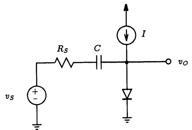
Fig. P3.7
3.7. For the circuit shown in Fig. P3.7 with Rs=1 kΩ, C=1.0 𝜇F, and I having several values of 1 mA, 0.1 mA, and 1 𝜇A, verify that the signal component in the output voltage for each case is given by:
Using Spice, simulate the transient behavior of this circuit with an input 100 Hz sine-wave signal of 1 mV-peak amplitude. Assume that the diode has model parameters IS=10 fA and n=2.
3.8. A voltage regulator consisting of two diodes in series fed with a constant current source is used as a replacement for a single carbon-zinc (battery) cell of nominal voltage 1.5 V. The regulator load current varies from 2 to 7 mA. Compare this regulator circuit for three different current source levels of 5, 10 and 15 mA as the load current varies over its full range. What is the change in the output voltage for each case? Assume that the diodes have a 0.7 V drop at a 1 mA current and n=2.
3.9. A zener shunt regulator of the type shown in Fig. 3.14 has been designed to provide a regulated voltage of about 10 V. The zener diode is of the type 1N4740 which is specified to have a 10 V drop at a test current of 25 mA. At this current its rz=7 Ω. The raw supply available has a nominal value of 20 V but can vary by as much as ±25%. The regulator is required to supply a load current of 0 to 20 mA. Assuming that the minimum zener current is to be 5 mA, the resistance R was determined to be 200 Ω. Using Spice, simulate the behavior of this circuit and:
(a) Find the load regulation. By what percentage does VO change from the no-load to full-load condition?
(b) Find the line regulation. What is the change in VO expressed as a percentage, corresponding to the ±25% change in VS.
(c) What is the maximum current that the zener diode has to conduct? What is maximum zener power dissipation?
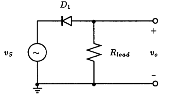
Fig. P3.10
3.10. For the half-wave rectifier circuit of Fig. P3.10. Let vS be a sinusoid with a 10 V-peak amplitude and let R=1 kW. Assume that diode has diode parameters IS=100 pA and n=1.679. Using Spice:
(a) Calculate and plot the transfer characteristic.
(b) Calculate and plot the output voltage waveform assuming that the input signal frequency is 1 kHz. Estimate the average value of this output signal.
(c) Determine the peak current in the diode.
(d) Determine the PIV of the diode.
3.11. Consider a half-wave rectifier circuit with a triangular input of 20 V peak-to-peak amplitude and zero average. The resistance in series with the diode is 1 kΩ. Assume that the diode has model parameters IS=100 pA and n=1.679. Calculate the output voltage and estimate the average value of this output signal.
Fig. P3.12
3.12. It is required to design a full-wave rectifier circuit using the circuit of Fig. P3.12 to provide an average output voltage of:
(a) 10 V.
(b) 100 V.
In each case find the required turns ratio of the transformer assuming LP=10 mH and check your results using Spice. Assume that the diodes are of the 1N4148 type, the ac line voltage is 120 V-rms and has a source resistance of 0.5 Ω.
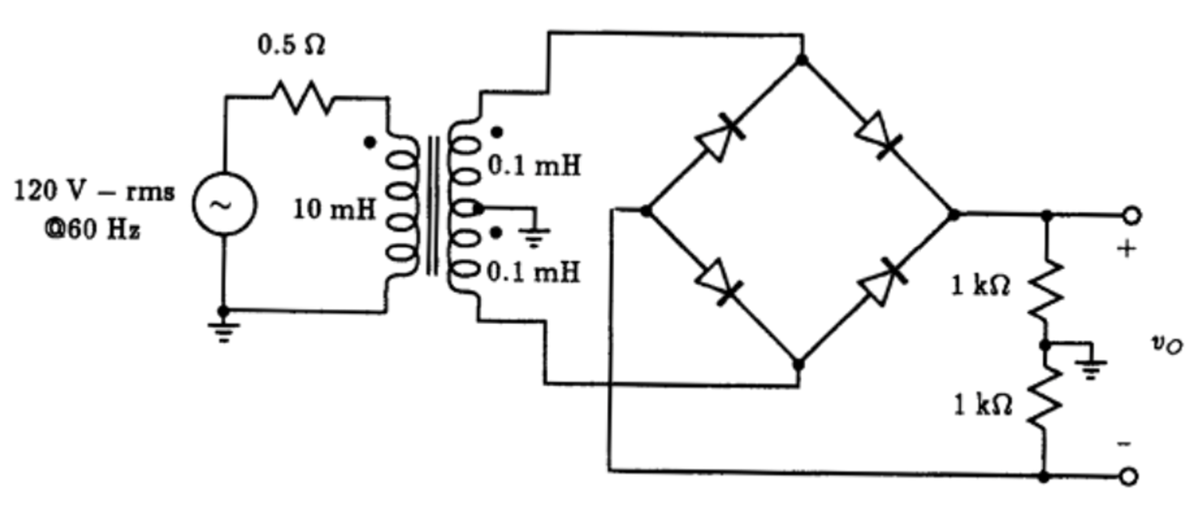
Fig. P3.13
3.13. The circuit in Fig. P3.13 implements a complementary-output rectifier. Simulate the behavior of this circuit using Spice and plot the voltage that appears across the two output terminals. Assume that the diodes have model parameters IS=100 fA and n=2. What is the PIV of each diode?
3.14. Design a half-wave peak rectifier circuit that provides an average DC output voltage of 15 V on which a maximum ±1 V ripple is allowed. The rectifier feeds a load of 150 Ω and the rectifier is fed from the line voltage (120 V-rms at 60 Hz) through a transformer. The diodes are assumed of the type 1N4148. Simulate the operation of your design using Spice and verify that it indeed satisfies the design requirements.
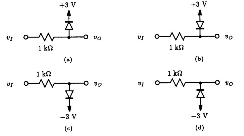
Fig. P3.15
3.15. Using Spice, plot the transfer characteristic vO versus vI for the four limiter circuits shown in Fig. P3.15. Assume that the diodes have model parameters IS=100 fA and n=1.6.
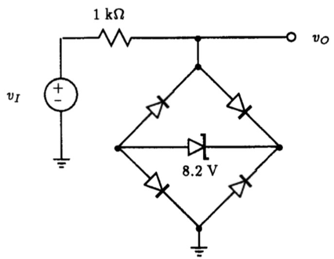
Fig. P3.16
3.16. Using Spice, plot the transfer characteristic vO versus vI of the circuit in Fig. P3.16 for -20 V ≤ vI ≤ +20 V. Assume that the diodes have model parameters IS=100 fA and n=1.6, and that the zener diode has a reverse-bias voltage drop of 8.2 V at a current of 10 mA and rz=20 Ω.
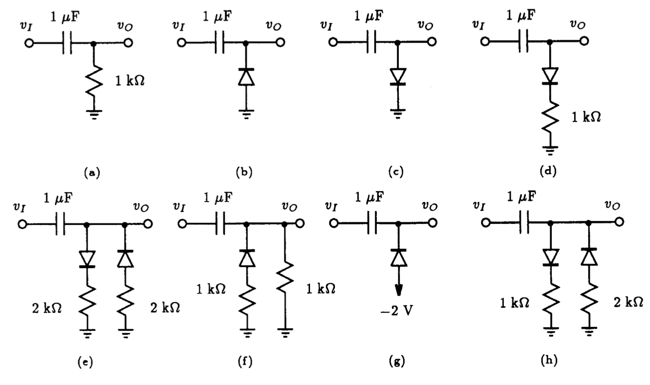
Fig. P3.17
3.17. For the circuits in Fig. P3.17, each utilizing diodes of the 1N4148 type, plot the output waveform of the circuit for a 10 V-peak amplitude input square-wave having a frequency of 1 kHz.