Chapter 4
Bipolar Junction Transistors (BJTs)
Gordon W. Roberts,
Department of Electrical & Computer Engineering, McGill University
In the previous chapter we outlined how the semiconductor diode is described to Spice using a diode element and model statement. Further, we illustrated how the terminal characteristics of a diode are modeled within Spice and how the user can alter the parameters of this model to more closely characterize specific diode behavior. In this chapter on the bipolar junction transistor (BJT) we shall proceed in a similar fashion, first outlining the two statements that are required to describe a BJT to Spice. This will then be followed by a brief description of the model used to represent the BJT within Spice. On completion of this, we shall use LTSpice to investigate the low-frequency behavior of various types of electronic circuits containing BJTs. The types of circuits that will be simulated will range from single npn and pnp transistor amplifiers to multiple-transistor amplifier circuits, as well as circuits that utilize the transistor as an on-off switch.
4.1 Describing BJTs To Spice
Two statements are required to describe any particular semiconductor device to LTSpice. One statement is necessary to describe the nature of the semiconductor device and the manner in which it is connected to the rest of the network, and the other statement is required to describe the parameters of the built-in model of the semiconductor device described by the first statement. In the following we shall describe these two statements as they apply to the BJT.
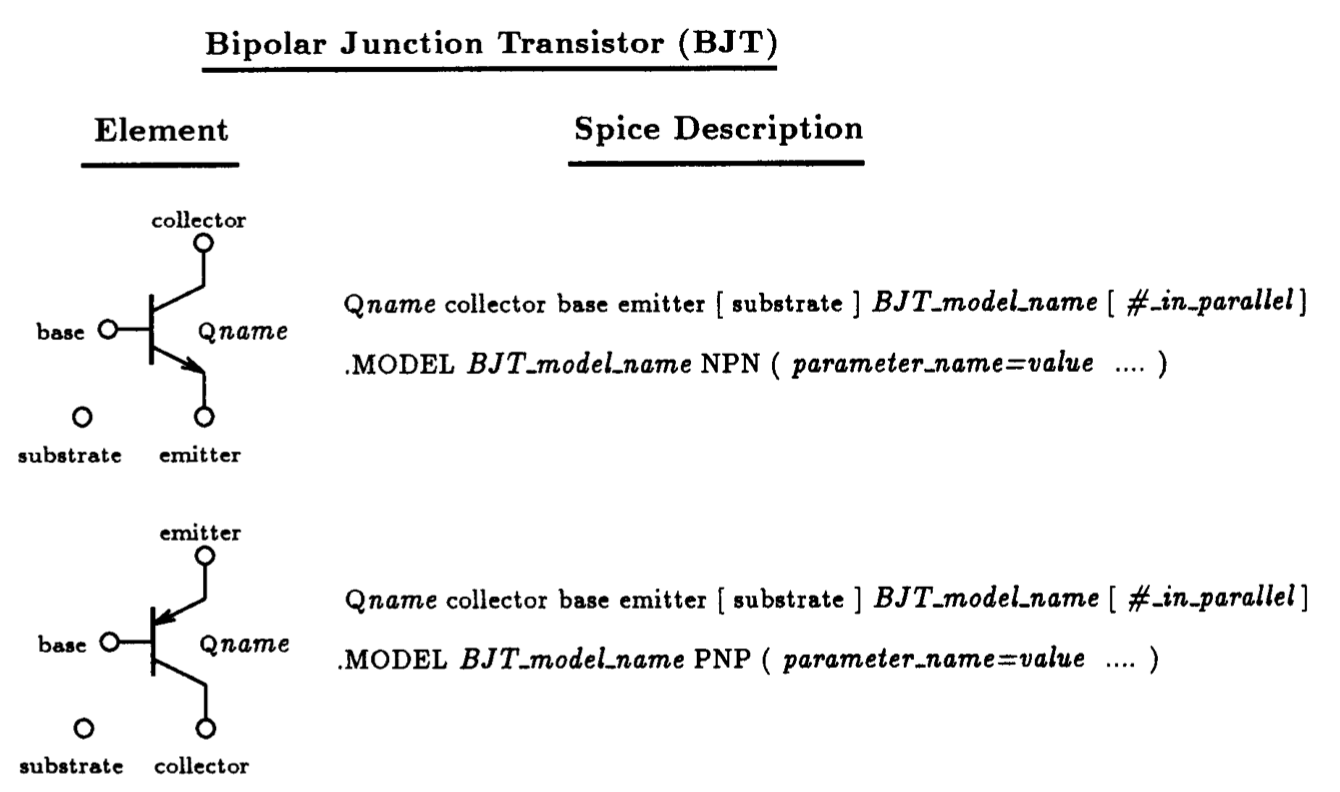
Fig. 4.1: Spice element description for the npn and pnp BJT. Also listed is the general form of the associated BJT model statement. A partial listing of the parameter values applicable to either the npn or pnp BJT given in Table 4.1.
4.1.1 BJT Element Description
The presence of a BJT in a circuit is described to Spice through the Spice input file using an element statement beginning with the letter Q. If more than one transistor exists in a circuit, then a unique name must be attached to Q to uniquely identify each transistor. This is then followed by a list of the three nodes to which the collector, base, and emitter of the BJT are connected to. One can also include the node that the substrate is connected to if it is an integrated transistor. Subsequently, on the same line, the name of the model that will be used to characterize this particular BJT is given. The name of this model must correspond to the name given on a model statement containing the parameter values that characterize this transistor to Spice. Lastly, one has the option of specifying the number of BJTs that are considered to be connected in parallel.
For quick reference we depict the syntax for the Spice statement describing the BJT in Fig. 4.1. Also shown is the syntax for the model statement (.MODEL) that must be present in any Spice input file that makes reference to the built-in BJT model of Spice. This statement defines the terminal characteristics of the BJT by specifying the values of particular parameters of the BJT model. We shall discuss the model statement more fully next.
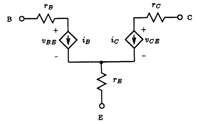
Fig. 4.2: The Spice large-signal BJT model for DC analysis.
4.1.2 BJT Model Description
As is evident from Fig. 4.1, the model statement for either the npn or pnp transistor begins with the keyword .MODEL and is followed by the name of the model used by a BJT element statement, the nature of the BJT (i.e., npn or pnp), and a list of the parameters characterizing the terminal behavior of the BJT, enclosed between brackets. The number of parameters associated with the Spice model of the BJT is rather large (40 in total), and their individual meanings are rather involved. Instead of trying to describe the meaning of each parameter of the BJT model, we shall simply outline the parameters of the Spice BJT model that are relevant to the discussion contained within this chapter.
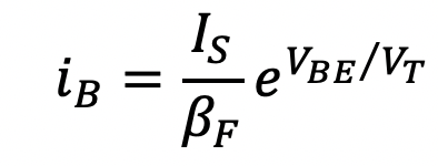
The Spice BJT model is illustrated schematically in Fig. 4.2. The ohmic resistances of the base, collector, and emitter regions of the BJT are lumped into three linear resistances rB, rC and rE, respectively. The DC characteristics of the intrinsic BJT are determined by the nonlinear dependent current sources iB and iC. The exact functional descriptions of these two currents - as adopted by Spice - are rather complex and will not be given here. Interested readers can consult [Nagel, 1975] for more details. For a transistor operated in its active mode, a first-order representation of these two currents can be described by the following two equations
(4.1)
and
(4.2)
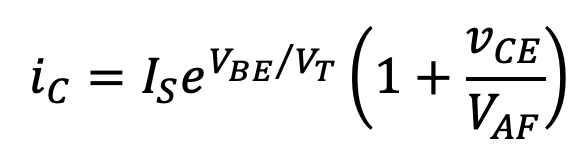
Here IS is the saturation current (similar to the diode saturation current) and VT is the thermal voltage (at 27 degree-C, equivalent to 25.89 mV). The constant βF is the forward common-emitter current gain. In many undergraduate electronics textbooks, this constant is designated simply as β. Spice attaches the subscript F to distinguish βF from another current gain βR which represents the common-emitter current gain of the same transistor when operated in the reverse mode (that is, with the emitter and collector interchanged). Finally, VAF is the forward early voltage (often denoted as VA).
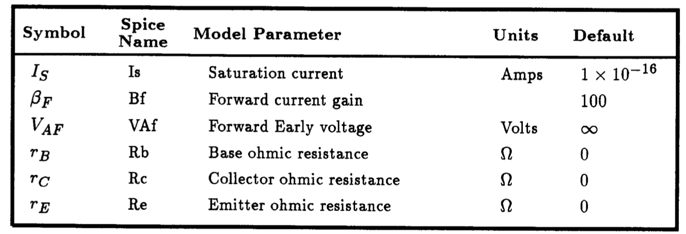
Table 4.1: A partial listing of the Spice parameters for a static BJT model.
A partial listing of the parameters associated with the Spice BJT model under static conditions is given in Table 4.1. Also listed are the associated default values; if the value of a particular parameter is not specified on the .MODEL statement, the parameter assumes its default value. To specify a parameter value one simply writes, for example, Is=1e-14, Bf=100, etc..
4.1.3 Verifying NPN Transistor Circuit Operation
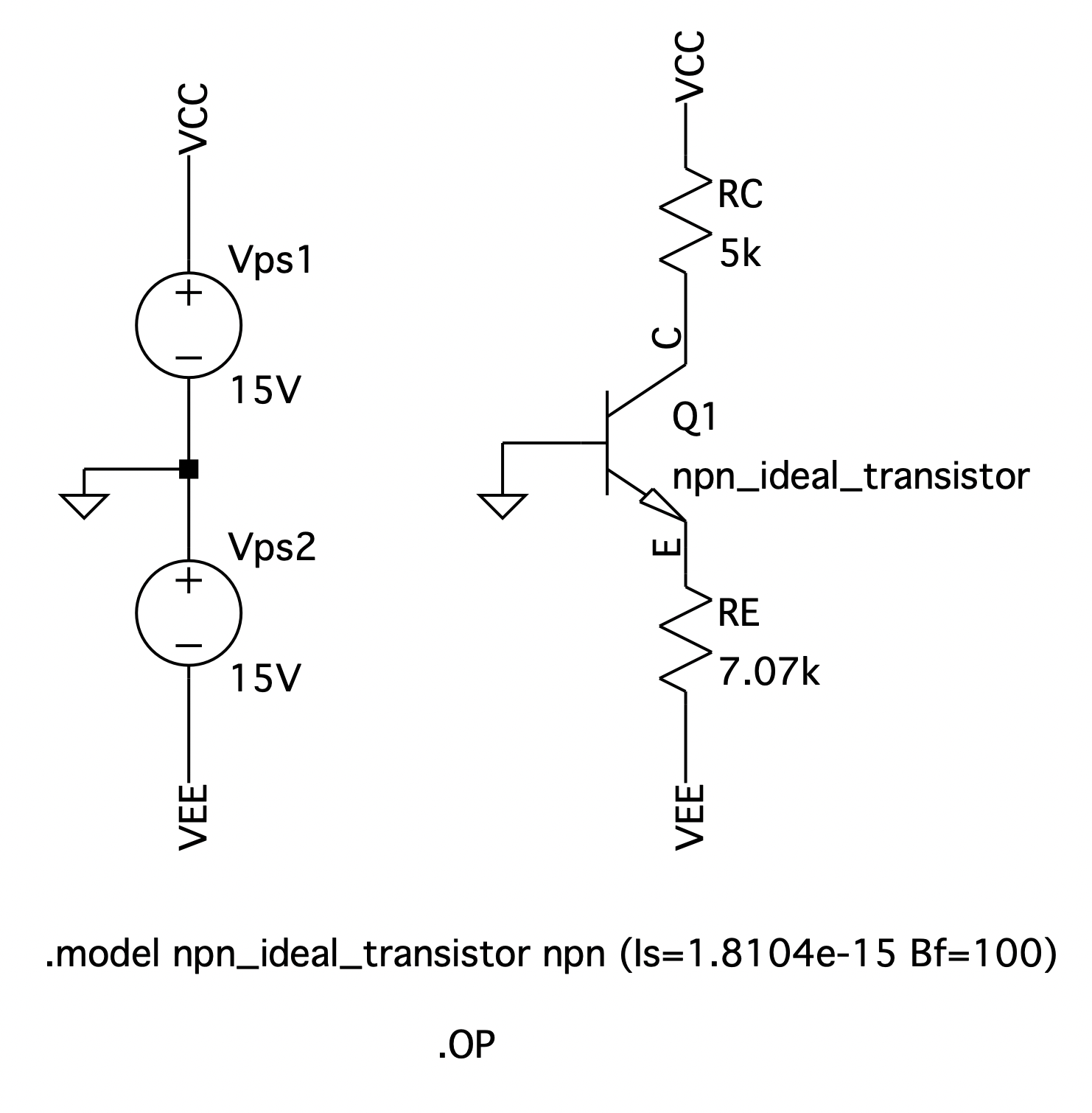
As the first example of this chapter, consider verifying the npn transistor shown in Fig. 4.3. This particular transistor circuit was designed to have a collector current of 2 mA and a collector voltage of +5 V.
For the purpose of design, the npn transistor was assumed to have a βF = 100 and to exhibit a vBE of 0.7 V at iC = 1 mA. The first condition can be directly specified on the BJT model statement using βF=100, however, the latter condition needs to be translated into a BJT parameter. From Eqn. (4.2) we can write
(4.3)
![]()
Now, to make matters simpler, we shall assume that VAF = infinity, thus reducing the above equation to
(4.4)
![]()
We can then solve to obtain IS=1.8104 x 10⁻¹⁵ A. Our model statement for this particular transistor is then described to LTSpice using the following statement:
.model npn_ideal_transistor npn (Is=1.8104e-15 Bf=100) .
Notice that we did not specify the value of VAF in the list of parameters, rather, we are relying on the default value assigned to VAF. Of course, the same could have also been done for the parameter βF.
|
Fig. 4.3: Transistor BJT amplifier circuit captured by LTSpice. LTSpice is used to calculate the DC operating point of this circuit assuming a simple model of BJT operation.
|
Example 4.1: Verifying Transistor Circuit Design * * Circuit Description * Vps1 VCC 0 15V Vps2 0 VEE 15V Q1 C 0 E 0 npn_ideal_transistor RC VCC C 5k RE E VEE 7.07k * transistor model statement .model npn_ideal_transistor npn (Is=1.8104e-15 Bf=100) · unused model statements that appear by default of accessing BJT .model NPN NPN .model PNP PNP .lib /Users/roberts/Library/Application Support/LTspice/lib/cmp/standard.bjt * * Analysis Requests * * calculate DC bias point information .OP .backanno .end
Fig. 4.4: The LTSpice generated circuit netlist for calculating the collector current and voltage of the transistor circuit shown in Fig. 4.3.
|
Assuming the nodes of the circuit are labeled as shown in Fig. 4.3, the corresponding LTSpice generated netlist (with some rearrangements) is listed in Fig. 4.4. An operating point analysis command (.OP) is included in the command window as seen in Fig. 4.3 to tell Spice to calculate the DC operating point of this circuit. On execution, the following DC operating point information results:
|
Operating Bias Point Solution: V(vcc) 15 voltage V(c) 4.99906 voltage V(e) -0.717255 voltage V(vee) -15 voltage Ic(Q1) 0.00200028 device_current Ib(Q1) 2.00028e-05 device_current Ie(Q1) -0.00202029 device_current I(Re) 0.00202019 device_current I(Rc) 0.00200019 device_current I(Vps2) -0.00202019 device_current I(Vps1) -0.00200019 device_current
|
As is evident, the collector of the transistor is at 4.99906 V and the collector current IC is 2.000 mA. Although, the collector voltage is not exactly at +5 V, the deviation from this value is extremely small (1 mV). If one were to back-track to find why this error occurred, one would find that the value of VT=25 mV assumed during the design phase is different than the value of VT=25.89 mV that LTSpice used, assuming a circuit temperature of 27°C. Repeating the design procedure with the exact value of VT=25.89 mV would result in an emitter resistance of RE=7.0703 k-ohm and a collector voltage much closer to +5 V.
4.2 Using LTSpice as a Curve Tracer
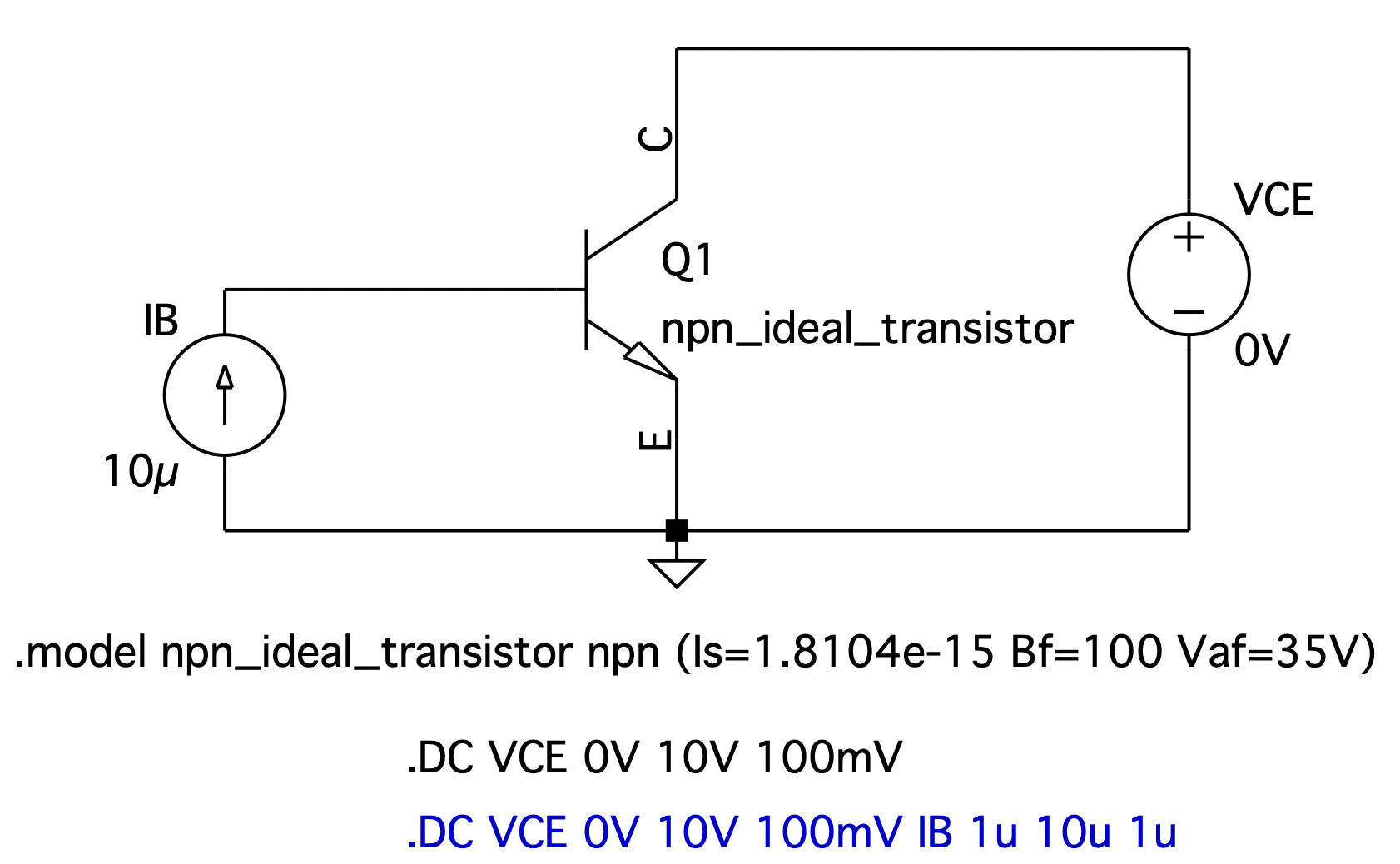
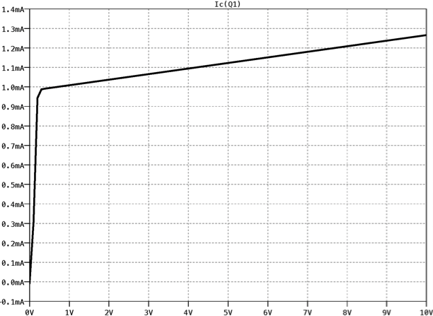
A typical curve-tracer arrangement for measuring the iC - vCE characteristics of a transistor is illustrated in Fig. 4.5 as captured by LTSpice. Here two independent sources vCE and iB are varied, and the collector current of the transistor is calculated. The collector current would then be plotted as a function of vCE and iB. For example, consider plotting the forward iC - vCE characteristics of a npn transistor characterized by IS=1.8104 x 10⁻¹⁵ A, βF=100, and a forward Early voltage VAF=35 V, for a base current of 10 𝜇A. The corresponding LTSpice generated circuit netlist for this particular situation can be seen listed in Fig. 4.6. Here a DC Sweep command is used to vary the collector-emitter voltage of transistor Q1 from 0 V to +10 V in 100 mV steps. The resulting iC - vCE characteristic as calculated by LTSpice is displayed in Fig. 4.7.
|
Fig. 4.5: LTSpice curve-tracer arrangement for calculating the iC - vCE characteristics of a BJT.
|
LTSpice As A Curve Tracer: BJT I-V Characteristics * * Circuit Description * VCE C 0 0V IB 0 N001 10µ * device under test Q1 C N001 0 0 npn_ideal_transistor * transistor model statement .model npn_ideal_transistor npn (Is=1.8104e-15 Bf=100 Vaf=35V) * * Analysis Requests * * vary Vce from 0V to 10V in steps of 100mV .DC VCE 0V 10V 100mV *.DC VCE 0V 10V 100mV IB 1u 10u 1u * unused model statements that appear by default of accessing BJT .model NPN NPN .model PNP PNP .lib /Users/roberts/Library/Application Support/LTspice/lib/cmp/standard.bjt .backanno .end
Fig. 4.6: The LTSpice generated circuit netlist for calculating the collector current of the transistor ci rcuit shown in Fig. 4.5 for a given base current and collector-emitter voltage.
|
|
Fig. 4.7: The iC - vCE curve at a base current of 10 uA for a transistor characterized by IS=1.8104 x 10⁻¹⁵ A, BF=100, and VAF=35 V.
|
Fig. 4.8: A family of iC - vCE curves for a base current varied between 1 uA and 10 uA in steps of 1 uA for a transistor characterized by IS=1.8104 x 10⁻¹⁵ A, BF=100, and VAF=35 V.
|
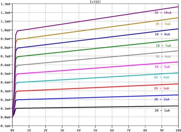
Typically, one also wants to vary the base current iB while at the same time varying vCE of the transistor. This can be accomplished with LTSpice by augmenting the DC Sweep command with another source name and the range of values it should be stepped through. For example, the DC Sweep command required to sweep vCE from 0 V to +10 V in 100 mV steps while at the same time sweeping iB from 1 𝜇A to 10 𝜇A in 1 𝜇A steps is simply achieved by changing the Spice directive command to the following:
.DC Vce 0V +10V 100mV Ib 1u 10u 1u.
In essence, this command tells LTSpice to perform the voltage sweep for each value specified by the current sweep. (For those familiar with computer programming, this command should remind them of a set of programming loops: the inner sweep being nested within the outer sweep.). The result of this analysis is displayed in Fig. 4.8. Clearly, other arrangements of the two independent sources are possible, thus allowing one to investigate other characteristics of the transistor. We encourage the reader to investigate some of them using the approach just outlined.
4.3 LTSpice Analysis of Transistor Circuits At DC
It is now time to investigate the DC operating point of several simple transistor circuits using LTSpice. Throughout this section we shall assume that the transistor is characterized by a βF=100, exhibits a vBE of 0.7 V at iC=1 mA, and that its Early voltage is infinite. The primary goal of this section is to determine, with the aid of Spice, the mode of operation that a transistor is working in.
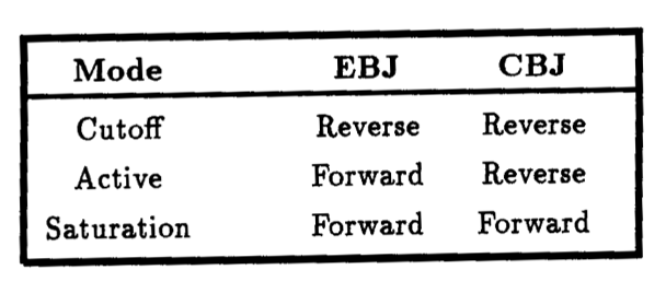
Table 4.2: BJT modes of operation.
4.3.1 Transistor Modes of Operation
Depending on the bias condition imposed across the emitter-base junction (EBJ) and the collector-base junction (CBJ), different modes of operation of the BJT are obtained, as shown in Table 4.2. In the following we shall look at several transistor circuits and use LTSpice to determine the mode of operation of each.
|
Fig. 4.9: A simple npn transistor circuit whose BJT is assumed to be operating in the active region.
|
NPN Transistor Operated In Active Mode * * Circuit Description * Vps1 VCC 0 10V Vps2 0 VEE 0V Vps3 VBB 0 4V Q1 C VBB E 0 npn_ideal_transistor RC VCC C 4.7k RE E VEE 3.3k * transistor model statement .model npn_ideal_transistor npn (Is=1.8104e-15 Bf=100) * unused model statements that appear by default of accessing BJT .model NPN NPN .model PNP PNP .lib /Users/roberts/Library/Application Support/LTspice/lib/cmp/standard.bjt * * Analysis Requests * * calculate DC bias point information .OP .backanno .end
Fig. 4.10: The Spice input file for calculating the DC operating point of the circuit shown in Fig. 4.9.
|
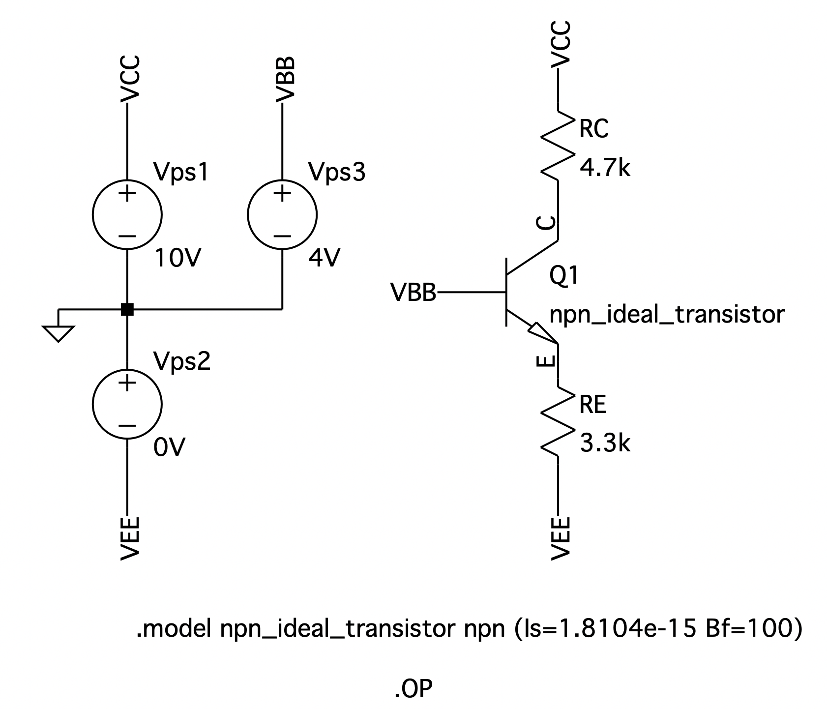
Active Region
Consider the circuit captured by LTSpice in Fig. 4.9 and the corresponding circuit netlist in Fig. 4.10. This same circuit was analyzed using a hand analysis; here transistor Q1 was shown to be operating in its active region. With the aid of an .OP command in LTSpice, the mode of this transistor will be determined.
The results of the .OP analysis are listed below:
|
Semiconductor Device Operating Points: --- Bipolar Transistors --- Name: q1 Model: npn_ideal_transistor Ib: 9.90e-06 Ic: 9.90e-04 Vbe: 6.99e-01 Vbc: -1.35e+00 Vce: 2.04e+00
Operating Bias Point Solution: V(vcc) 10 voltage V(c) 5.34523 voltage V(vbb) 4 voltage V(e) 3.30093 voltage V(vee) 0 voltage Ic(Q1) 0.000990382 device_current Ib(Q1) 9.90382e-06 device_current Ie(Q1) -0.00100029 device_current I(Re) 0.00100028 device_current I(Rc) 0.000990377 device_current I(Vps3) -9.90377e-06 device_current I(Vps2) -0.00100028 device_current I(Vps1) -0.000990377 device_current
|
Included amongst the list of node voltages is a partial summary of the DC operating point conditions associated with the transistor. This includes the currents IB and IC, and the voltages VBE, VBC, and VCE. Other information is included in this list of operating point information but is not shown here. Also, we do not show the small-signal parameters associated with the hybrid-pi model of the transistor, deferring discussion of this topic to a later stage.
What one should notice here, amongst this operating point information, is that the base-emitter junction is forward biased with VBE=0.699 V and the collector-base junction is reversed biased with VBC=-1.35 V; thus, confirming that transistor Q1 is indeed operating in its active region. One could have deduced this same information from the DC node voltages, but for multiple transistor circuits this can be a tedious endeavor. Also, the collector and base currents agree reasonably well with the values calculated by hand analysis.
Saturation Region
If we increase the base voltage of the circuit of Fig. 4.9 from +4 V to +6 V, transistor Q1 leaves the active region and moves into the saturation region. To see this, change the value of Vps3 shown in Fig. 4.10 to +6 V and re-run the LTSpice analysis. The results found in the log file are:
|
Semiconductor Device Operating Points: --- Bipolar Transistors --- Name: q1 Model: npn_ideal_transistor Ib: 6.03e-04 Ic: 9.97e-04 Vbe: 7.19e-01 Vbc: 6.85e-01 Vce: 3.39e-02
Operating Bias Point Solution: V(vcc) 10 voltage V(c) 5.31469 voltage V(vbb) 6 voltage V(e) 5.28075 voltage V(vee) 0 voltage Ic(Q1) 0.000996903 device_current Ib(Q1) 0.000603359 device_current Ie(Q1) -0.00160026 device_current I(Re) 0.00160023 device_current I(Rc) 0.000996875 device_current I(Vps3) -0.000603353 device_current I(Vps2) -0.00160023 device_current I(Vps1) -0.000996875 device_current
|
As is evident, both VBE and VBC are forward biased, suggesting that Q1 is operating in its saturation region. The BJT saturation region of operation will be studied further in Sections 4.4 and 4.5.
Cutoff Region
Finally, if we reduce the base voltage to zero volts, then the transistor becomes cutoff. Altering the circuit schematic to reflect this (i.e., setting Vps3=0) and re-running the LTSpice analysis, results in the following following:
|
Semiconductor Device Operating Points: --- Bipolar Transistors --- Name: q1 Model: npn_ideal_transistor Ib: -1.00e-11 Ic: 1.00e-11 Vbe: -5.97e-12 Vbc: -1.00e+01 Vce: 1.00e+01
Operating Bias Point Solution: V(vcc) 10 voltage V(c) 10 voltage V(vbb) 0 voltage V(e) 5.97432e-12 voltage V(vee) 0 voltage Ic(Q1) 1.00036e-11 device_current Ib(Q1) -1.00018e-11 device_current Ie(Q1) -1.8104e-15 device_current I(Re) 1.8104e-15 device_current I(Rc) 1.00036e-11 device_current I(Vps3) 1.00018e-11 device_current I(Vps2) -1.8104e-15 device_current I(Vps1) -1.00036e-11 device_current |
Here, both VBE and VBC are reversed biased, indicating that Q1 is now cutoff. Notice, however, that even under cutoff conditions the transistor is still conducting a base and collector current (and, of course, an emitter current). These currents are mainly leakage currents associated with the two reverse biased junctions of the transistor.
|
Fig. 4.11: A simple pnp transistor circuit. |
PNP Transistor DC Operating Point Calculation * * Circuit Description * Vps1 VCC 0 10V Vps2 0 VEE 10V Vps3 VBB 0 0V RE VCC E 2k RC C VEE 1k Q1 C VBB E 0 pnp_ideal_transistor * transistor model statement .model pnp_ideal_transistor pnp (Is=1.8104e-15 Bf=100) * unused model statements that appear by default of accessing BJT .model NPN NPN .model PNP PNP .lib /Users/roberts/Library/Application Support/LTspice/lib/cmp/standard.bjt * * Analysis Requests * * calculate DC bias point information .OP .backanno .end
Fig. 4.12: The Spice input file for calculating the DC operating point of the circuit shown in Fig. 4.11.
|
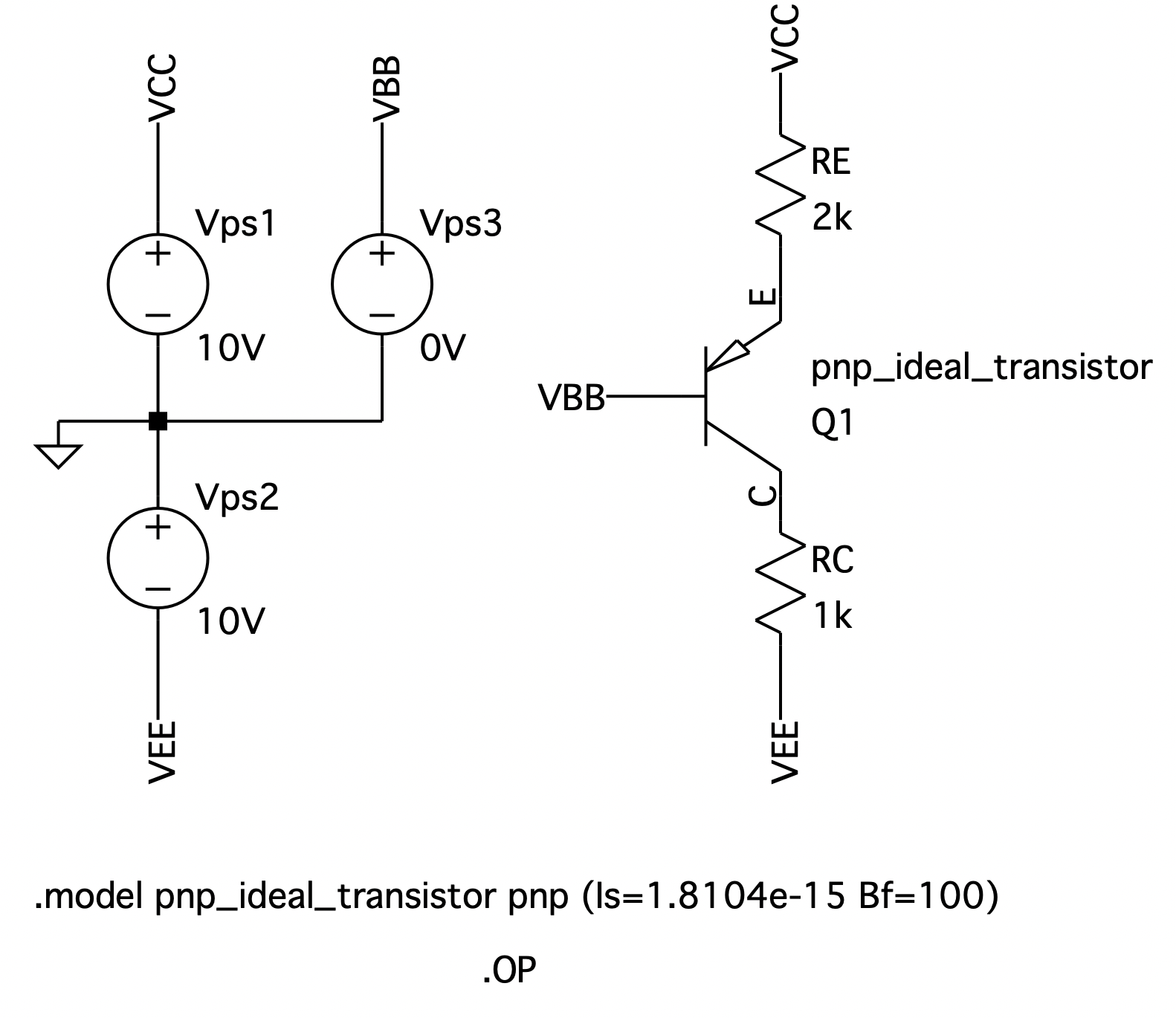
4.3.2 Computing DC Bias of a PNP Transistor Circuit
The above circuit examples consisted of npn transistors only. In this next example we shall calculate the DC operating point of a circuit containing a pnp transistor. As far as LTSpice is concerned, pnp transistor circuits are no more complicated than npn transistor circuits.
Consider the circuit captured by LTSpice shown in Fig. 4.11. The LTSpice generated circuit netlist for this circuit arrangement with a .OP Spice directive can be seen listed in Fig. 4.12. The results of this DC analysis are shown below:
|
Semiconductor Device Operating Points: --- Bipolar Transistors --- Name: q1 Model: pnp_ideal_transistor Ib: -4.58e-05 Ic: -4.58e-03 Vbe: -7.39e-01 Vbc: 5.42e+00 Vce: -6.15e+00
Operating Bias Point Solution: V(vcc) 10 voltage V(e) 0.738709 voltage V(c) -5.4152 voltage V(vee) -10 voltage V(vbb) 0 voltage Ic(Q1) -0.0045848 device_current Ib(Q1) -4.5848e-05 device_current Ie(Q1) 0.00463065 device_current I(Rc) 0.0045848 device_current I(Re) 0.00463065 device_current I(Vps3) 4.5848e-05 device_current I(Vps2) -0.0045848 device_current I(Vps1) -0.00463065 device_current
|
From the above results, it is obvious that the transistor is operating in the active mode. Notice that the polarity of the transistor currents is opposite to those of a npn transistor operating in its active region (see the previous subsection). Further, one should also note that Spice defines a positive collector current of a pnp transistor as the current flowing into the collector. When one compares the above LTSpice results with those generated by a simple hand calculation, one find we are in very good agreement; about a 0.4% difference.
In the above analysis, the Early effect was neglected. In practise this is never the case. In the following, let us repeat the above analysis assuming the pnp transistor has an Early voltage VAF of 100 V. We shall then compare the resulting transistor collector current with that obtained previously when the Early effect was ignored. Consider replacing the transistor model statement for the pnp transistor given in the schematic circuit of Fig. 4.11 with the following one:
.model pnp_ideal_transistor pnp (Is=1.8104e-15 Bf=100 Vaf=100V).
Re-running the LTSpice DC analysis, one finds in the log output file the following results:
|
Semiconductor Device Operating Points: --- Bipolar Transistors --- Name: q1 Model: pnp_ideal_transistor Ib: -4.35e-05 Ic: -4.59e-03 Vbe: -7.37e-01 Vbc: 5.41e+00 Vce: -6.15e+00
Operating Bias Point Solution: V(vcc) 10 voltage V(e) 0.737362 voltage V(c) -5.4122 voltage V(vee) -10 voltage V(vbb) 0 voltage Ic(Q1) -0.0045878 device_current Ib(Q1) -4.35224e-05 device_current Ie(Q1) 0.00463132 device_current I(Rc) 0.0045878 device_current I(Re) 0.00463132 device_current I(Vps3) 4.35224e-05 device_current I(Vps2) -0.0045878 device_current I(Vps1) -0.00463132 device_current
|
Here one can see that the collector current is now 4.59 mA. This is in contrast to the previous situation when the Early effect was ignored, and the LTSpice analysis revealed a collector current of 4.58 mA. In the latter case, a similar result would also be obtained by a simple hand calculation, as was noted above. Thus, if we compare the result obtained by Spice with the Early effect included to that obtained by a simple hand calculation, we see a difference of about 0.2%. For most practical engineering situations, a 5% to 10% accuracy obtained from a simple hand analysis is usually quite acceptable. But, more importantly, to account for the Early effect during hand analysis would complicate the analysis significantly that it would probably mask any insight. Thus, if greater accuracy is thought necessary then one should make use of a detailed LTSpice analysis with the transistor Early effect included.
|
(a)
(b)
Fig. 4.13: A multiple transistor circuit: (a) schematic, and (b) LTSpice captured circuit schematic with transistor model statements and .OP Spice directive included.
|
Multiple Transistor Circuit Bias Point Calculation * * Circuit Description * Vps1 VCC 0 15V Vps2 0 VEE 0V * npn stage Q1 C1 B1 E1 0 npn_ideal_transistor RC1 VCC C1 5k RE1 E1 VEE 3k RB1 VCC B1 100k RB2 B1 VEE 50k * pnp stage Q2 C2 C1 E2 0 pnp_ideal_transistor RE2 VCC E2 2k RC2 C2 VEE 2.7k * transistor model statement .model npn_ideal_transistor npn (Is=1.8104e-15 Bf=100 Vaf=100V) .model pnp_ideal_transistor pnp (Is=1.8104e-15 Bf=100 Vaf=100V) * unused model statements that appear by default of accessing BJT .model NPN NPN .model PNP PNP .lib /Users/roberts/Library/Application Support/LTspice/lib/cmp/standard.bjt * * Analysis Requests * * calculate DC bias point information .OP .backanno .end
Fig. 4.14: The Spice input file for calculating the DC operating point of the multiple transistor circuit shown in Fig. 4.13.
|
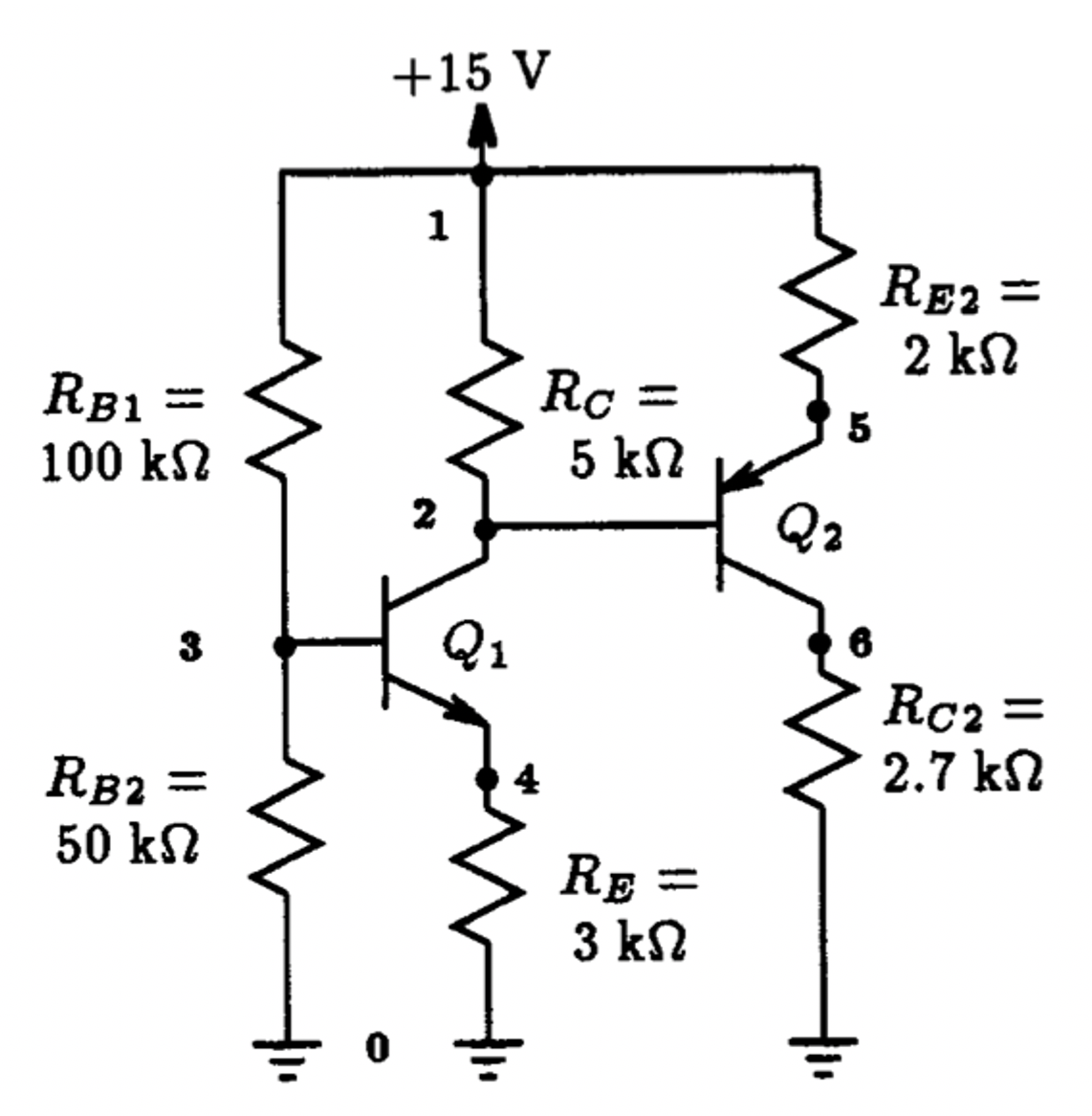
4.3.3 DC Operating Point of a Multiple Transistor Circuit
Consider the multiple transistor circuit shown in Fig. 4.13(a). It involves both npn and pnp transistors. We shall compute the DC operating point of this circuit using LTSpice. The s hematic entered into LTSpice is shown in Fig. 4.13(b) with both the npn and pnp transistor models, together with a .OP Spice directive. The corresponding LTSpice generated circuit netlist is shown listed in Fig. 4.14. On completion of the DC analysis, the following results are obtain:
|
Semiconductor Device Operating Points: --- Bipolar Transistors --- Name: q1 q2 Model: npn_ideal_transistor pnp_ideal_transistor Ib: 1.28e-05 -2.73e-05 Ic: 1.28e-03 -2.73e-03 Vbe: 7.06e-01 -7.25e-01 Vbc: -4.18e+00 1.37e+00 Vce: 4.88e+00 -2.10e+00
Operating Bias Point Solution: V(vcc) 15 voltage V(e2) 9.47794 voltage V(c2) 7.38097 voltage V(vee) 0 voltage V(c1) 8.75261 voltage V(b1) 4.57439 voltage V(e1) 3.86875 voltage Ic(Q1) 0.00127682 device_current Ib(Q1) 1.27682e-05 device_current Ie(Q1) -0.00128958 device_current Ic(Q2) -0.00273369 device_current Ib(Q2) -2.73369e-05 device_current Ie(Q2) 0.00276103 device_current I(Rb2) 9.14879e-05 device_current I(Rb1) 0.000104256 device_current I(Re1) 0.00128958 device_current I(Rc1) 0.00124948 device_current I(Rc2) 0.00273369 device_current I(Re2) 0.00276103 device_current I(Vps2) -0.00411476 device_current I(Vps1) -0.00411476 device_current
|
Comparing these results with those calculated by hand, we see that the results generated by hand analysis (e.g., IC1= 1.28 mA and IC2= 2.75 mA) are quite close to the values generated by LTSpice. Moreover, we see that both transistors are operating in the active mode.
In the following we repeat the analysis with each transistor having an Early voltage of 100 V. This requires that we modify the two-transistor model statement given in the model statements of Fig. 4.13(b) to the following:
.model npn_ideal_transistor npn (Is=1.8104e-15 Bf=100 Vaf=100V)
.model pnp_ideal_transistor pnp (Is=1.8104e-15 Bf=100 Vaf=100V)
On doing so, and re-running the LTSpice analysis, we obtain the following results:
|
Semiconductor Device Operating Points: --- Bipolar Transistors --- Name: q1 q2 Model: npn_ideal_transistor pnp_ideal_transistor Ib: 1.23e-05 -2.71e-05 Ic: 1.28e-03 -2.75e-03 Vbe: 7.05e-01 -7.25e-01 Vbc: -4.13e+00 1.30e+00 Vce: 4.84e+00 -2.03e+00
Operating Bias Point Solution: V(vcc) 15 voltage V(e2) 9.44787 voltage V(c2) 7.42211 voltage V(vee) 0 voltage V(c1) 8.72272 voltage V(b1) 4.58944 voltage V(e1) 3.88473 voltage Ic(Q1) 0.00128259 device_current Ib(Q1) 1.23168e-05 device_current Ie(Q1) -0.00129491 device_current Ic(Q2) -0.00274893 device_current Ib(Q2) -2.71364e-05 device_current Ie(Q2) 0.00277607 device_current I(Rb2) 9.17888e-05 device_current I(Rb1) 0.000104106 device_current I(Re1) 0.00129491 device_current I(Rc1) 0.00125546 device_current I(Rc2) 0.00274893 device_current I(Re2) 0.00277607 device_current I(Vps2) -0.00413563 device_current I(Vps1) -0.00413563 device_current
|
Here we see that the collector current of Q1 remains at 1.28 mA, but the collector current of Q2 has increased to a level of 2.75 mA, a 0.02 mA increase. This example, like the previous one, demonstrates the effect that transistor Early voltage has on the DC bias levels in a circuit and shows that it is usually small. Thus, not accounting for it during a hand analysis seems reasonable.
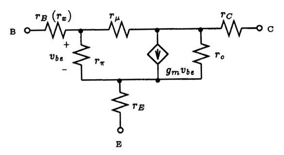
Fig. 4.15: The small-signal BJT Spice model under static conditions.
4.4 BJT Transistor Amplifiers
Transistors operated in their active region find important applications as linear amplifiers. Design and analysis of linear amplifiers is facilitated by the use of small-signal models for the BJT. In the following we discuss the small-signal model used by LTSpice.
4.4.1 BJT Small-Signal Model
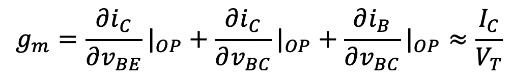
Under static and small-signal conditions, the linearized BJT Spice model is the familiar hybrid-pi model shown in Fig. 4.15. Both the npn and pnp transistor have the same hybrid-pi model, so we make no distinction between the two. The transconductance gm is related to the DC bias current IC according to the following
(4.5)
Similarly, the input and output resistances are also related to the transistors DC operating point, according to the following
(4.6)

(4.7)
and ru is approximated as
(4.8)
Also included in the hybrid-model are the ohmic resistances of the three junctions; rC, rB (rx), and rE. Note that rE is not the small-signal re used to describe the incremental emitter resistance.
The small-signal parameters of a transistor are usually computed by LTSpice prior to most analyses. In many types of analysis, the small-signal model of the BJT is paramount to the analysis. LTSpice will list the small-signal model parameters of all transistors in a given circuit when an .OP directive is specified. Because of the importance of the base resistance rB on small-signal operation, LTSpice will also list this value amongst the small-signal parameters in the output file. It will be denoted by Rx.
As an example of the small-signal parameters that are listed in the Spice output file as a result of an .OP analysis command, we show below the operating point information for transistors Q1 and Q2 in our previous example given in subsection 4.3.3:
|
--- Bipolar Transistors --- Name: q1 q2 Model: npn_ideal_transistor pnp_ideal_transistor Ib: 1.23e-05 -2.71e-05 Ic: 1.28e-03 -2.75e-03 Vbe: 7.05e-01 -7.25e-01 Vbc: -4.13e+00 1.30e+00 Vce: 4.84e+00 -2.03e+00 BetaDC: 1.04e+02 1.01e+02 Gm: 4.96e-02 1.06e-01 Rpi: 2.10e+03 9.53e+02 Rx: 0.00e+00 0.00e+00 Ro: 8.12e+04 3.69e+04 Cbe: 0.00e+00 0.00e+00 Cbc: 0.00e+00 0.00e+00 Cjs: 0.00e+00 0.00e+00 BetaAC: 1.04e+02 1.01e+02 Cbx: 0.00e+00 0.00e+00 Ft: 0.00e+00 0.00e+00
|
Here we see a list containing the DC operating point and small-signal model parameters for both the npn and pnp transistors in the circuit of Fig. 4.13. Besides the parameters that have already been explained, this list also contains other parameters, such as capacitances CBE, CBC, CBX and CJS. These capacitances model dynamic effects of the transistor and will be further explained in Chapter 7. Likewise, BETAAC, and FT, are parameters that are derived from the dynamic small-signal model of the transistor and will also be explained in Chapter 7.
|
(a)
(b)
Fig. 4.16: A simple common-emitter voltage amplifier: (a) schematic, and (b) LTSpice captured circuit schematic with transistor model statements and .OP Spice directive included.
|
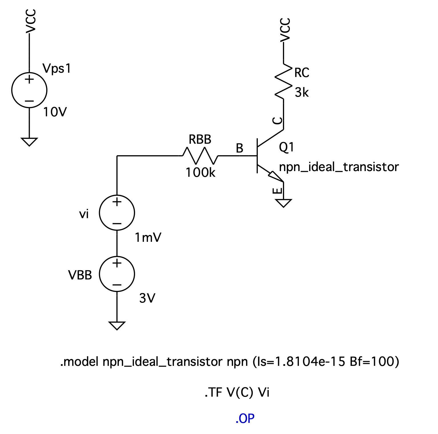
Calculating Voltage Gain Of A Transistor Amplifier * * Circuit Description * * dc supplies Vps1 VCC 0 10V VBB N002 0 3V * small-signal input vi N001 N002 1mV * amplifier circuit Q1 C B 0 0 npn_ideal_transistor RC VCC C 3k RBB B N001 100k * transistor model statement .model npn_ideal_transistor npn (Is=1.8104e-15 Bf=100) * unused model statements that appear by default of accessing BJT .model NPN NPN .model PNP PNP .lib /Users/roberts/Library/Application Support/LTspice/lib/cmp/standard.bjt * * Analysis Requests * * calculate small-signal transfer function: Vo/Vi .TF V(C) Vi * Later we shall also calculate the small-signal parameters of the transistor *.OP .backanno .end
Fig. 4.17: The Spice input file for calculating the small-signal voltage gain of the circuit shown in Fig. 4.16(b).
|
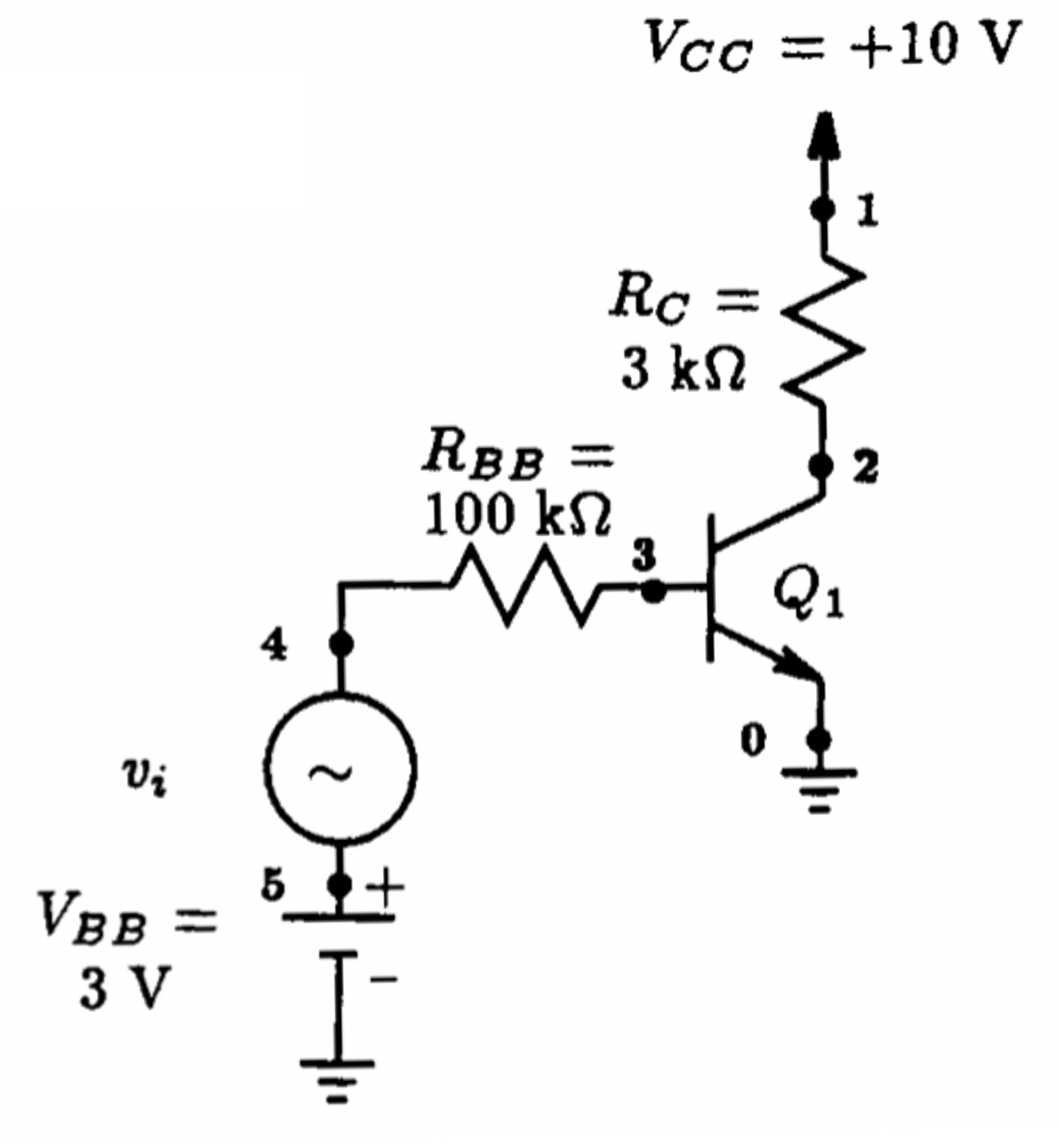
4.4.2 Single-Stage Voltage-Amplifier Circuits
Consider the voltage amplifier circuit shown in Fig. 4.16(a). Here we shall use LTSpice to calculate the voltage gain of this circuit assuming that the transistor has a βF = 100 and IS=1.8104 x 10⁻¹⁵ A. The other parameters of the BJT model will take on their default values. In Fig. 4.16(b) the schematic captured by LTSpice is shown. Here a small-signal transfer function analysis is requested using the .TF directive between the input source vi and the collector terminal of the transistor. A DC analysis is also listed using the .OP command but is left inactive as it is highlighted in blue. The data generated by the .OP analysis will allow one to cross-check the results found from a hand analysis. The LTSpice generated circuit netlist is shown in Fig. 4.17.
The results of the .TF command are displayed in graphical form as follow:
|
|
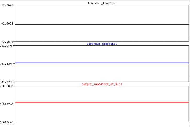
Here one can see that the voltage gain of this circuit is -2.966 V/V. Also, the input and output resistance of this circuit are 101.1 k-ohm and 3 k-ohm, respectively. Referring back to the circuit shown in Fig. 4.16, these resistance levels seem to be in line with what one would expect.
We can collaborate the voltage gain calculation found using the .TF command by evaluating the voltage gain of the amplifier found through a small-signal analysis (assuming transistor output resistance is infinite), i.e.,
(4.9)
![]()
To find the small-signal parameters of the npn transistor, a DC analysis using the .OP directive is performed and a partial listing of the operating point information is shown below:
|
Name: q1 Model: npn_ideal_transistor Ib: 2.28e-05 Ic: 2.28e-03 Vbe: 7.21e-01 Vbc: -2.44e+00 Vce: 3.16e+00 BetaDC: 1.00e+02 Gm: 8.82e-02 Rpi: 1.13e+03 Rx: 0.00e+00 Ro: 1.25e+54
|
From the above list, we see that gm=88.2 mA/V and rp=1.13 k-ohm. Substituting these values, together with RC=3 k-ohm and RBB=100 k-ohm, into Eqn. (4.9), one finds the voltage gain to be -2.96 V/V. Comparing this result with that computed using the .TF command of Spice, as expected, one finds almost exact agreement. The difference is due the number of significant digits used in the two calculations. In principle, these two calculations should be in perfect agreement because the .TF command calculates the voltage gain in the exact same way.
|
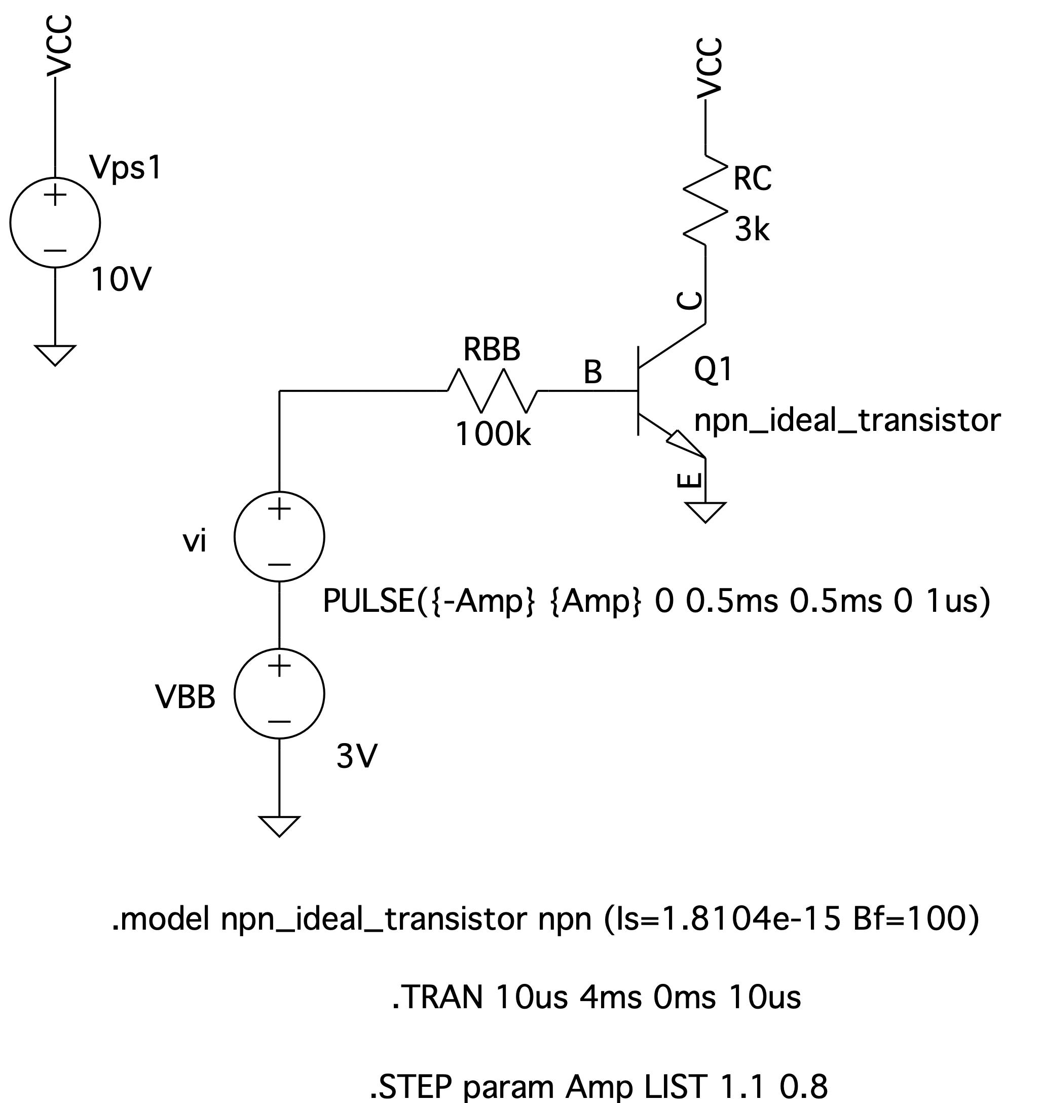
Fig. 4.18: LTSpice captured circuit schematic with dynamic triangular input signal. A .STEP command will direct LTSpice to analysis the transient response for two separate triangular input signals of amplitudes 1.1 V and 0.8 V.
|
Calculating Output Signal Of A Transistor Amplifier * * Circuit Description * * dc supplies Vps1 VCC 0 10V VBB N002 0 3V * triangular input vi N001 N002 PULSE({-Amp} {Amp} 0 0.5ms 0.5ms 0 1us) * amplifier circuit Q1 C B 0 0 npn_ideal_transistor RC VCC C 3k RBB B N001 100k * transistor model statement .model npn_ideal_transistor npn (Is=1.8104e-15 Bf=100) * unused model statements that appear by default of accessing BJT .model NPN NPN .model PNP PNP .lib /Users/roberts/Library/Application Support/LTspice/lib/cmp/standard.bjt * * Analysis Requests * .TRAN 10us 4ms 0ms 10us .STEP param Amp LIST 1.1 0.8 .backanno .end
Fig. 4.19: The LTSpice generated circuit netlist for calculating the amplifier response (Fig. 4.18) subject to a triangular waveform input with two separate amplitudes of 1.1 V and 0.8 V. .
|
|
|
|
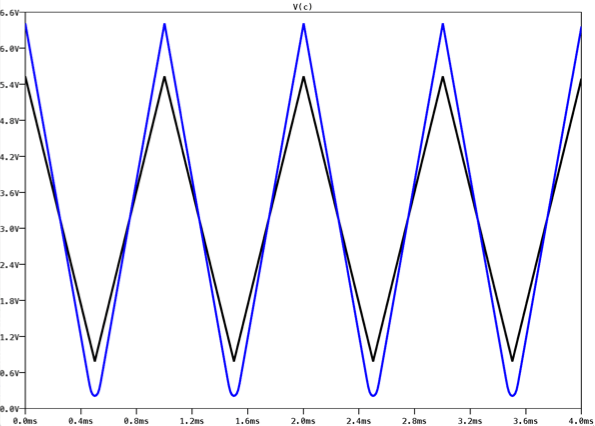
Fig. 4.20: The output voltage waveform of the amplifier shown in Fig. 4.18 for two different inputs levels of 0.8 V and 1.1 V. The larger output signal is seen to be clipped on its lower peaks.
|
To visualize the operation of this amplifier, consider simulating the circuit shown in Fig. 4.16 with a time-varying input. More specifically, we shall consider that vi is time-varying with a triangular waveform. We shall consider that the input signal has a period of 1 ms and an input amplitude of 1.1 V. Moreover, we shall repeat the same example with the input amplitude reduced to 0.8 V. We shall then want to compare the results.
To emulate the first triangular waveform, we could set the input signal as a PULSE source with the following parameters:
Vi 4 5 PULSE (-1.1V 1.1V 0 0.5ms 0.5ms 0 1ms)
The rise and fall times are set to equal half the period of the triangle waveform of 1 ms. The pulse width field is set to zero. A transient analysis is then run. Subsequently, the amplitude of the triangular wave would be reduced to 800 mV with the following PULSE statement:
Vi 4 5 PULSE (-0.8V 0.8V 0 0.5ms 0.5ms 0 1ms)
and the transient analysis is run again. As a matter of convenience, and one that will allow the two signals to be superimposed on the same graph, a .STEP directive will be used, together with the triangular amplitude set by a global variable called Amp. As always, this variable Amp will be enclosed between brackets to force substitution before execution. The source statement will then be written as
Vi 4 5 PULSE ({-Amp} {Amp} 0 0.5ms 0.5ms 0 1ms)
and the .STEP command written as
.STEP param Amp LIST 1.1V 0.8V
Furthermore, we added a .TRAN statement to calculate the time response of the circuit over a 4 ms interval using the following directive:
.TRAN 10us 4ms 0ms 10us
The resulting circuit schematic captured by LTSpice can be seen in Fig. 4.18 and the corresponding circuit netlist can be seen listed in Fig. 4.19.
The voltage waveforms at the collector of the amplifier for both input levels, as calculated by LTSpice, are displayed in Fig. 4.20. Both signals are riding on a DC component of 3.2 V, corresponding to the DC bias point at the collector. One will also notice that the larger output waveform is clipped on its lower peak. This can be traced back to the transistor being forced into its cutoff region when the input signal level exceeds a 0.82 V level. The other waveform does not appear to be clipped, confirming that the transistor stays out of its cutoff region.
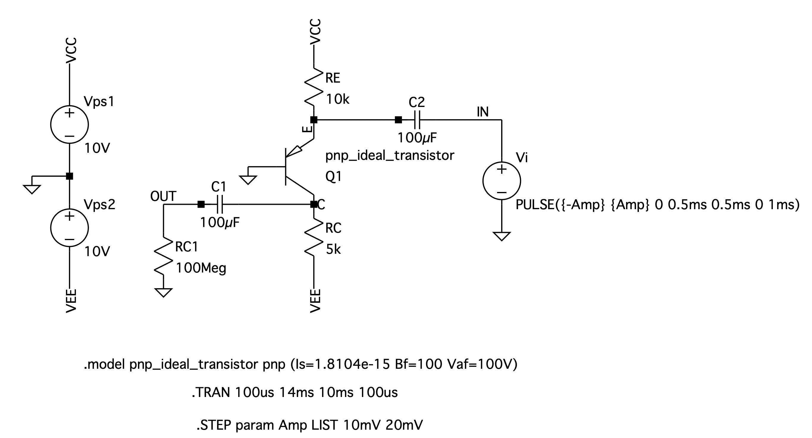
|
(a)
(b)
Fig. 4.21: A pnp transistor amplifier circuit: (a) schematic, and (b) LTSpice captured circuit schematic with transistor model statement, .STEP and .TRAN Spice directive included.
|
Time-Domain Waveforms For A PNP Transistor Amplifier
** Circuit Description ** * dc supplies V+ 1 0 DC +10V V- 5 0 DC -10V * small-signal triangular-wave input Vi 3 0 PULSE (-10mV 10mV 0 0.5ms 0.5ms 0 1ms) * amplifier circuit Q1 4 0 2 pnp_transistor Rc 4 5 5k Re 1 2 10k * dc blockers - very large capacitors C1 3 2 100uF IC=-0.6972V C2 4 6 100uF IC=-5.3946V * output node (very large resistance as not to load the amplifier) Ro 6 0 100Meg * transistor model statement .model pnp_transistor pnp (Is=1.8104e-15 Bf=100) ** Analysis Requests ** * calculate transient response using initial conditions .TRAN 100us 14ms 10ms 100us UIC ** Output Requests ** .PLOT TRAN V(4) V(3) .probe .end
Fig. 4.22: The LTSpice generated circuit netlist for calculating the amplifier response (Fig. 4.21) subject to a triangular waveform input with two separate amplitudes of 10 mV and 20 mV.
|
|
|
|
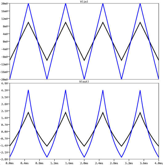
Fig. 4.23: Input and output waveforms of the pnp amplifier shown in Fig. 4.21. The top graph displays the two input triangular waveforms and the bottom graph displays the output response to the two input signals. Distortion is evident in both output waveforms.
|
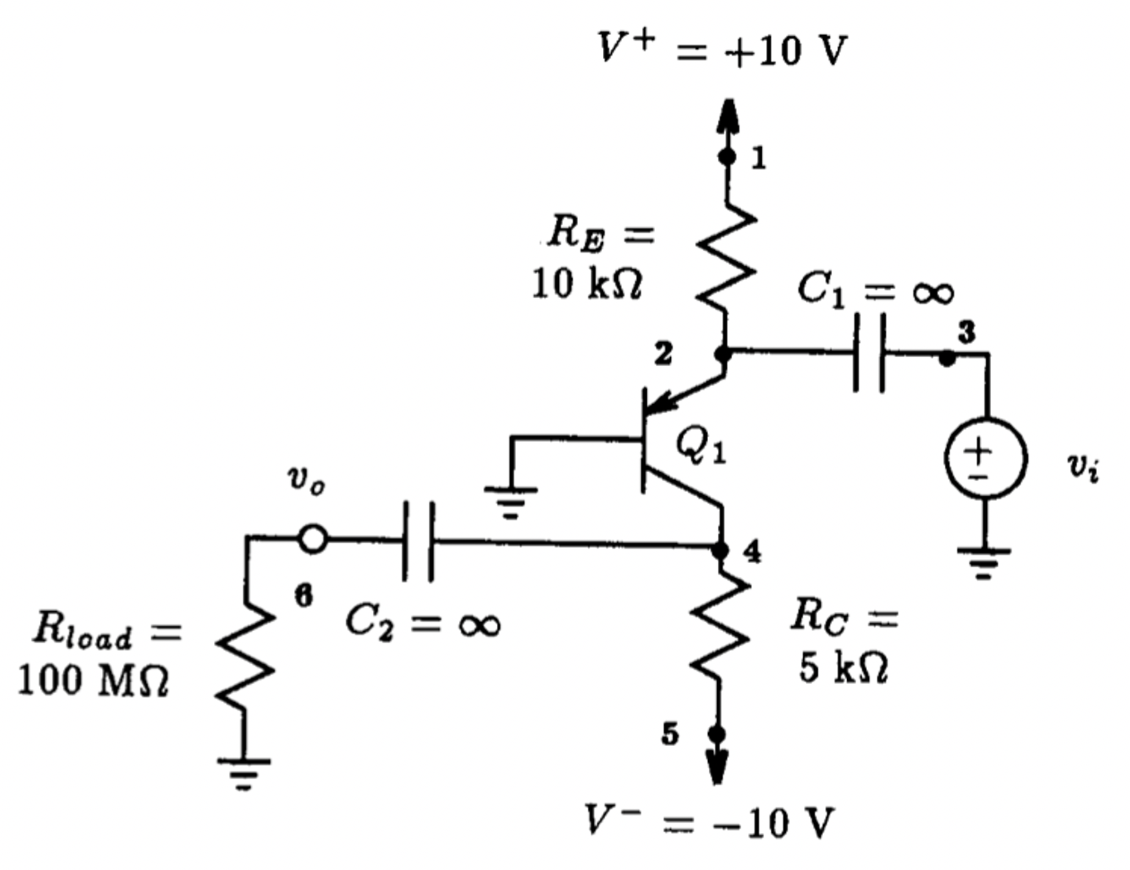
Another Example:
As another example of a transistor being used to form a linear amplifier, consider the circuit shown in Fig. 4.21. In this particular case, a pnp transistor is the central component of the design. From a hand analysis, the amplifier is found to have a noninverting voltage gain of 183.3 V/V. Moreover, as the input signal is applied directly across the base-emitter junction of the pnp transistor, the input signal amplitude must remain below 10 mV to justify small-signal operation and obtain this large voltage gain. In the following we shall simulate the amplifier circuit shown in Fig. 4.21(a) subject to a triangular waveform input signal having a peak value of 10 mV and compare it to one with twice the amplitude at 20 mV. Once again, a .STEP directive will be used to compare the two results, along with assigning a global variable to set the amplitude of the triangular input set by the PULSE generator. The schematic captured by LTSpice is shown in Fig. 4.21(b) and the corresponding circuit netlist is listed in Fig. 4.22. The infinite-valued capacitors, C1 and C2, are represented in the circuit schematic of Fig. 4.21(b) by large 100 𝜇F capacitors. As these large capacitors require a large time to charge, the transient analysis will run from time zero but only print out the results after a 10 ms delay. This will enable us to focus on the steady-state behavior. The transient analysis will be specified using the .TRAN directive
.TRAN 100us 14ms 10ms 100us
and the input signal amplitude varied using the following .STEP directive
.STEP param Amp LIST 10mV 20mV
Running the LTSpice analysis results in the plot of the input and output signals from the amplifiers as shown in Fig. 4.23 for the two input amplitudes. The larger output signal in the lower trace due to the 20-mV input signal clearly deviates from an ideal triangle waveform; it looks more parabolic than linear. The smaller output signal caused by the 10-mV input signal though much more linear, exhibits some deviation from the ideal, thus suggesting that the small-signal linear range of operation is actually less than 10 mV. We also see from Fig. 4.23 that for the 10-mV peak input signal, the corresponding output signal has a peak to peak excursion of 3.4 V, corresponding to a signal gain of 170 V/V. This result is, therefore, in reasonable agreement with the small-signal gain that was calculated by hand at 183.3 V/V.
|
|
Fig. 4.24: Basic single-stage BJT amplifier configurations: (a) common-emitter amplifier, (b) common-base amplifier and (c) common-collector amplifier. |
4.5 Basic Single-Stage BJT Amplifier Configurations
In this section, we shall investigate the three basic types of amplifier configurations shown in Fig. 4.24: the common-emitter (CE), common-base (CB) and common-collector (CC). The primary goal of this section is to determine the small-signal parameters of these amplifiers, such as input resistance Ri, output resistance Ro, voltage gain Av and current gain Ai, using the AC analysis facility of LTSpice. These results will then be compared to those predicted by the formulae derived by using a small-signal hand analysis. The transistor used in each amplifier of Fig. 4.24 will be assumed modeled after the commercial 2N2222 npn transistor.
|
(a)
|
(b) |
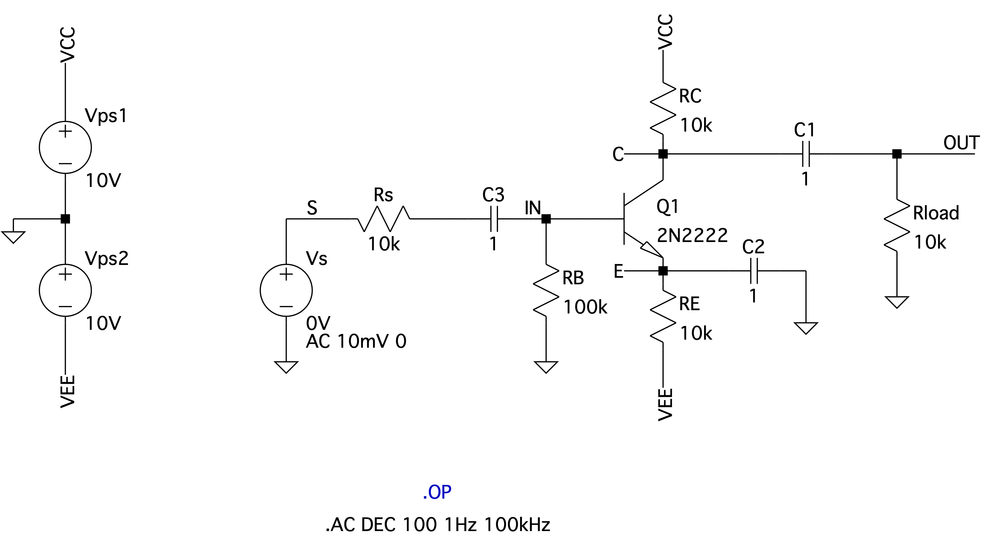
Fig. 4.25: (a) Circuit setup used to determine the amplifier's small-signal parameters: Av, Ai and Ri, and (b) LTSpice schematic capture with AC analysis directive activated.
|
(a)
|
(b)
|
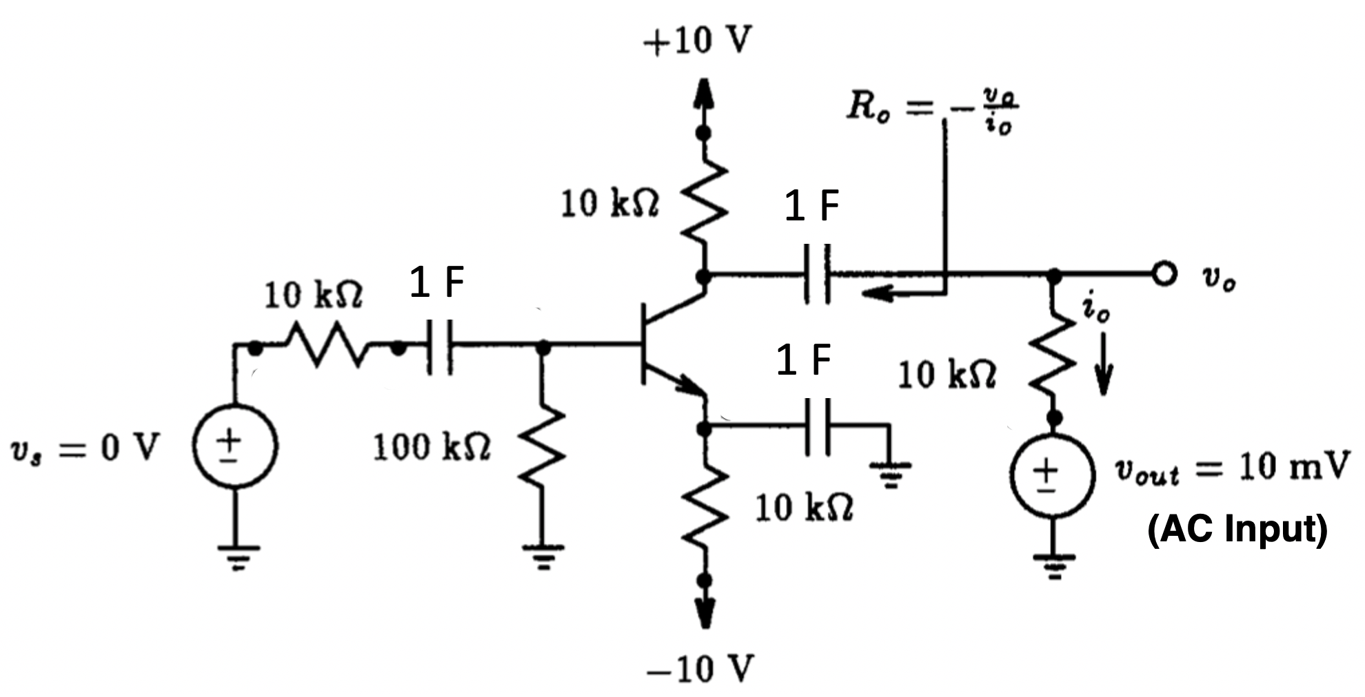
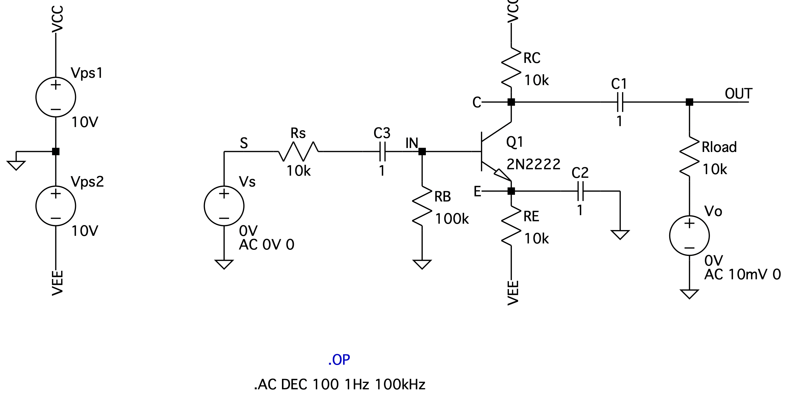
Fig. 4.26: (a) Circuit setup used to determine the amplifier's output resistance Ro, and (b) LTSpice schematic capture with AC analysis directive activated.
|
Fig. 4.27: The small-signal gain parameters of the common-emitter amplifier of Fig. 4.25. Top graph shows the midband voltage gain Av, middle graph shows the current gain Ai and the bottom graph shows the input amplifier resistance Rin. |
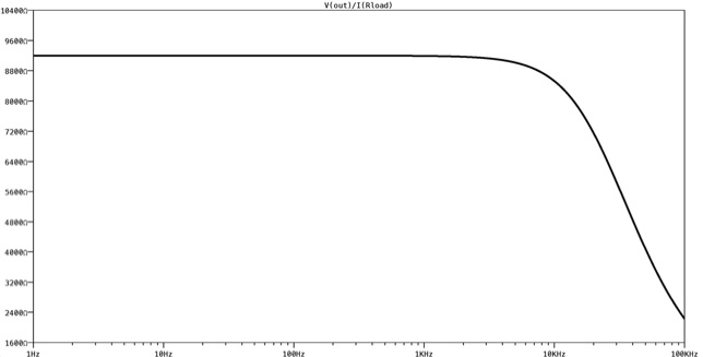
Fig. 4.34: The output resistance of the common-emitter amplifier of Fig. 4.26 as computed by LTSpice.
|
|
|
|
|
|
|
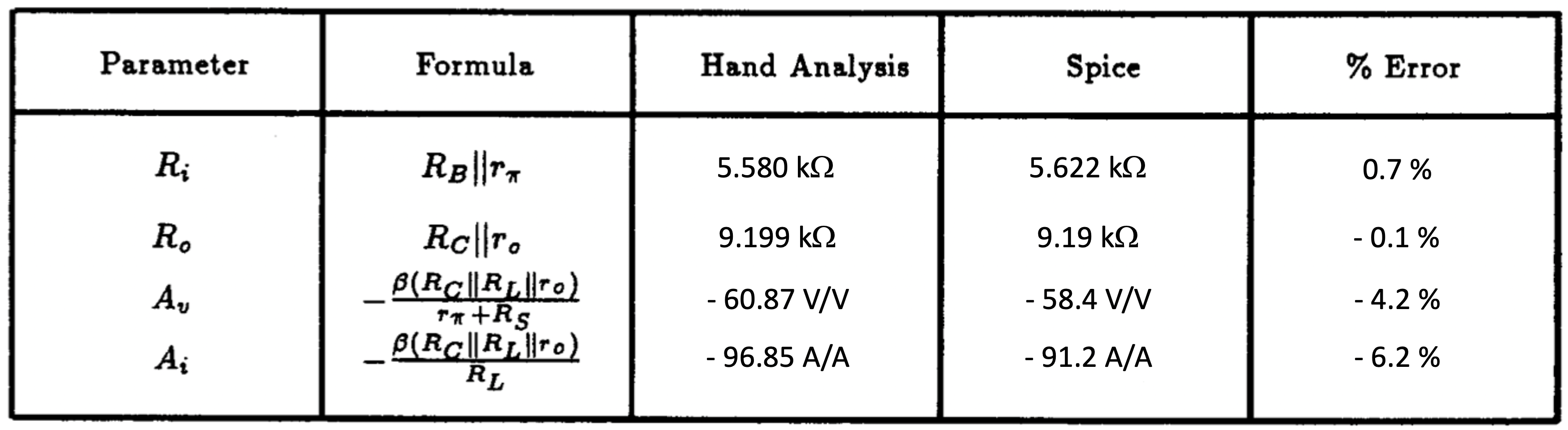
Table 4.4: Comparing the small-signal amplifier parameters of the common-emitter amplifier shown in Fig. 4.24(a) as calculated by hand analysis and that indirectly computed using LTSpice.
|
The Common-Emitter Amplifier
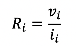
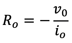
As the first example of this section, let us compute the small-signal parameters of the common-emitter (CE) amplifier shown in Fig. 4.24(a). To obtain all four parameters, i.e., Av, Ai, Ri and Ro, we will have to run two separate LTSpice analyses; one for computing the input current and the output voltage for a known voltage applied to the input of the amplifier, and the other for computing the current supplied by a voltage source connected to the output terminal of the amplifier when the input voltage source is set to zero. These two situations are depicted in Fig. 4.25 and 4.26. The input current to the amplifier can be determine by monitoring the current supplied by the input voltage source vs or the current flowing through the source resistor Rs. The four parameters of the amplifier can then be computed from these results according to the following:
(4.12)
(4.13)
(4.14)
(4.15)
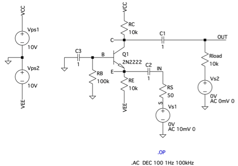
For the first case depicted in Fig. 4.25(a), consider applying a 10 mV AC signal to the input of the amplifier. A DC input voltage signal would not be useful here since the input source to the amplifier is AC-coupled. Thus, the frequency of the input signal should be selected to be in the midband frequency range of the amplifier, deemed to be from 1 Hz to 10 kHz. With the choice of decoupling and by-pass capacitors selected here (each selected very large at 1 F – please note that if one adds the F for Farad with the capacitor value then LTSpice will interpret the values as 10-12 Farads, resulting in an incorrect simulation), input frequencies from 1 Hz to 10 kHz is sufficiently midband. The circuit schematic captured by LTSpice is shown in Fig. 4.25(b). Both a DC and an AC analysis requests are specified; albeit, the DC analysis is commented out for the time being. The results of the AC analysis will be used to indirectly calculate the small-signal gain parameters of the amplifier, as mentioned above. The results of the DC analysis will provide us with the small-signal parameters of the transistor from which we can use small-signal formulae to predict the small-signal parameters of the amplifier and compare them to those computed by the indirect AC analysis approach. The AC analysis request a sweep of the input frequencies from 1 Hz to 100 kHz.
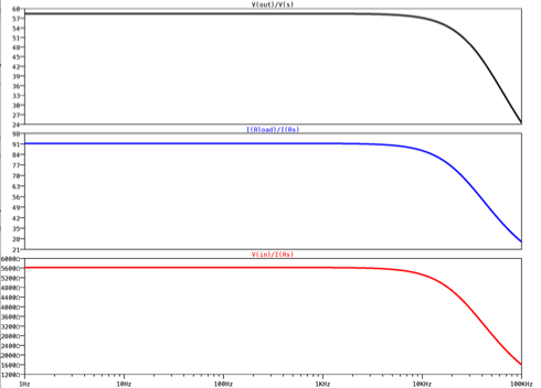
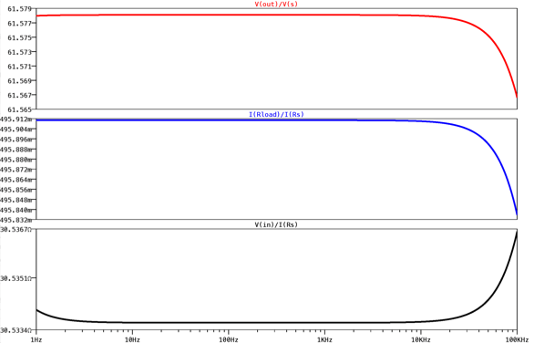
Executing the AC analysis results in the three graphs shown in Fig. 4.27. The top graph shows the ratio of the output voltage to the source voltage level over the mid-band range of the amplifier (1 Hz – 10 kHz), thus the amplifier has a voltage gain Av of magnitude 58.4 V/V (as found by the waveform viewer). The middle graph shows the midband current gain Ai of this amplifier to have a magnitude of 91.2 A/A, and the bottom graph show the input resistance to the amplifier to be 5622 ohms.
Repeating this same process but with the input voltage source level set to 0 V and the level of the voltage source in series with the load resistance set to 10 mV AC, we can determine the output resistance of this amplifier. This requires that we modify the LTSpice schematic capture as shown in Fig. 4.26(b). Here the input AC source is set to 0 V (AC) and another 10 mV AC voltage source is included in series with the load resistance. The results of the AC analysis are shown in Fig. 4.28 where the output resistance Ro is found to be 9.19 k-ohm.
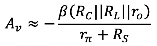
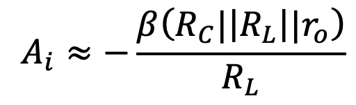
To compare the above results with those predicted by hand analysis, we list below the expressions for Av, Ai, Ri and Ro in terms of the small-signal model parameters of the transistor:
(4.16)
![]()
(4.17)
![]()
(4.18)
(4.19)
Here β is the small-signal transistor current gain[1] defined in terms of gm and rp according to:
(4.20)
![]()
Referring back to the command window for the circuit captured in Fig. 25(b), the AC analysis command was deactivated and the .OP directive was activated so that the dc operating point information can be found for the 2N2222 transistor, Q1. On execution, the following device information was found in the SPICE Error Log file:
|
--- Bipolar Transistors --- Name: q1 Model: 2n2222 Ib: 4.38e-06 Ic: 8.87e-04 Vbe: 6.52e-01 Vbc: -1.57e+00 Vce: 2.22e+00 BetaDC: 2.03e+02 Gm: 3.42e-02 Rpi: 5.91e+03 Rx: 1.00e+01 Ro: 1.15e+05
|
Substituting the appropriate parameter value, together with values for the different circuit components, we find: Av=-60.9 V/V, Ai=-96.9 A/A, Ri=5.580 k-ohm and Ro=9.199 k-ohm. To compare these with those computed indirectly by LTSpice above, we list in Table 4.4 a comparison of the results of these two approaches. The first and second column of this table list the small-signal parameters of the amplifier and its formula in terms of the small-signal transistor model parameters. The third and fourth columns indicate the value predicted by hand analysis and that obtained indirectly with LTSpice. The fifth column indicates the relative difference between the two results as a means of indicating how accurate the hand analysis is. As is evident from the results listed in this table, the results compare quite well.
|
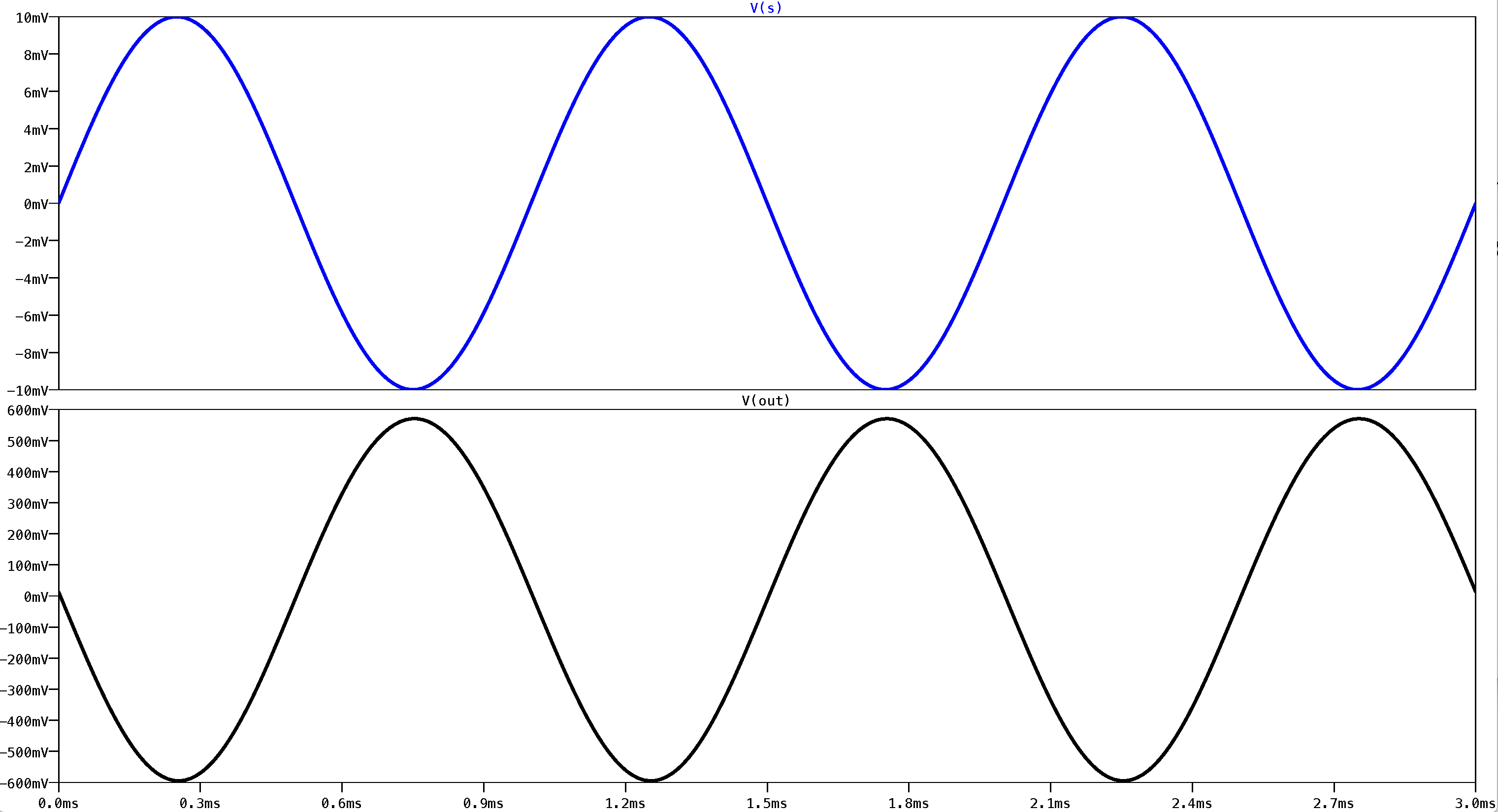
Fig. 4.29: Circuit setups used to determine the transient response of the CE amplifier subject to a 10 mV, 1 kHz sinusoidal signal. |
Fig. 4.30: The input and output time-varying voltage waveforms associated with the common-emitter amplifier shown in Fig. 4.29. |
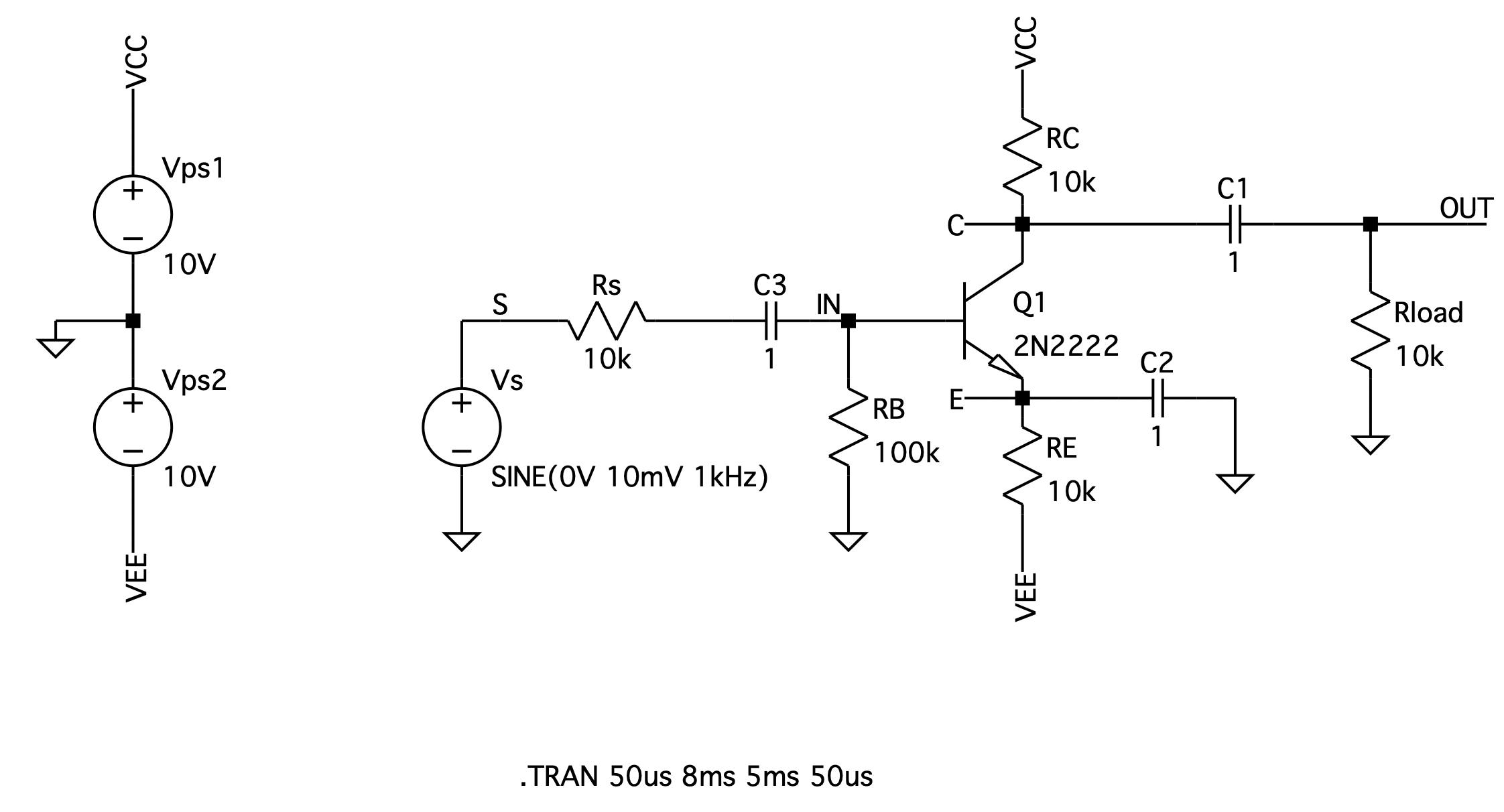
To demonstrate the usefulness of a small-signal analysis, let us apply a small-amplitude sinusoidal signal to the input of the amplifier and observe the time-varying signal that appears at the output of this amplifier. Say, for the sake of illustration, we apply a 10-mV sinusoidal of 1 kHz frequency to the input of the amplifier. The circuit captured by LTSpice for this particular situation is provided in Fig. 4.29. A transient analysis command is specified to compute the output waveform over three cycles of the input signal beginning at a time of 5 ms. This is to ensure that the circuit has had sufficient time to reach steady state. The dc-coupling and bypass capacitors have been assigned more practical values of 10 uF each, unlike those used in the previous AC analysis. In this way, the time to reach steady state is drastically reduced. One should note that by the very nature of a LTSpice transient analysis, the analysis performed here is a large-signal analysis and not a small-signal analysis even though the input signal level is small.
The results of the transient analysis are shown in Fig. 4.30. The top graph displays the 10-mV peak, 1 kHz input sinusoidal signal and the bottom graph displays the corresponding output signal. With the aid of the waveform viewer, the amplitude of the output signal is 570.1 mV. Thus, the voltage gain of this amplifier is seen to be about -57 V/V, which agrees with that predicted by the two analyses above.
|
Fig. 4.31: LTSpice schematic capture used to determine the common-based small-signal parameters: Av, Ai and Ri. Note that the input source level is set to 10 mV AC and the output source is set to 0 mV AC.
|
Fig. 4.32: The small-signal gain parameters of the common-base amplifier of Fig. 4.31. Top graph shows the midband voltage gain Av, middle graph shows the current gain Ai and the bottom graph shows the input amplifier resistance Rin. |
|
Fig. 4.33: LTSpice schematic capture used to determine the common-base amplifier's output resistance Ro. Note that the input AC source level is set to 0 V and the output source is set to 10 mV AC.
|
Fig. 4.34: The output resistance of the common-base amplifier of Fig. 4.33 as computed by LTSpice.
|
|
Table 4.5: Comparing the small-signal parameters of the common-base amplifier shown in Fig. 4.24(b) as calculated by hand analysis to those indirectly computed using LTSpice. |
The Common-Base Amplifier
Another important amplifier configuration is the common-base (CB) amplifier shown in Fig. 4.27(b). Here the base of the transistor is AC grounded, the input signal source is connected to the emitter, and the load is connected to the collector. In the following we shall repeat the analysis method carried out on the common-emitter amplifier using LTSpice and compare the results with those estimated by the small-signal formulas derived by hand analysis.
The common-base amplifier circuit captured by LTSpice is shown in Fig. 4.31. Two AC voltage sources can be seen, one at the input to the amplifier, one at its output. These sources will perform the same tasks as for the common-emitter amplifier seen previously. One will be set to 10 mV AC amplitude, while the other is set to 0 AC. Then, the roles will be reversed. Both a DC and an AC analysis are specified in the command window, however, the dc-analysis is deactivated for the time being. The AC analysis will enable us to determine the current supplied to the amplifier by the input voltage source, and the voltage and current supplied to the load resistor. Whereas the DC analysis will provide us with the small-signal model parameters of the transistor for hand analysis purposes.
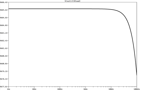
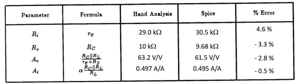
Submitting the LTSpice input file for processing results in the plot containing the three graphs in Fig. 4.31. Here one can see that the common-base amplifier has across the midband (100 Hz – 10 kHz) a gain of Av = 61.5 V/V, a current gain of Ai = 0.495 A/A and an input resistance of 30.5 ohms.
Repeating this same process but with the input voltage source level set to 0 V and the level of the voltage source in series with the load resistance increased to 10 mV AC, we find as plotted in Fig. 4.34 that the midband output resistance Ro of this amplifier is 9.68 k-ohm.
As a means of comparison, we summarize in Table 4.5 the small-signal formulae pertinent to the common-base amplifier, together with their values as calculated by substituting the relevant transistor small-signal model parameters into each equation. The small-signal model parameters for the 2N2222 transistor are identical to those found in the common-emitter case in the previous subsection. This is not too surprising given that the transistor of the common-base amplifier is biased in exactly the same manner as in the common-emitter amplifier. This was also confirmed by the DC analysis performed by LTSpice on the common-base amplifier. A fourth column is also included in this table listing the small-signal parameters computed from the LTSpice analysis above. As is evident from the fifth column, indicating the relative percent error between the two methods of estimating the amplifier small-signal parameters, we see that they are in very good agreement.
|
Table 4.6: Comparing the small-signal parameters of the common-collector amplifier shown in Fig. 4.24 (c) as calculated by hand analysis to those indirectly computed using LTSpice.
|
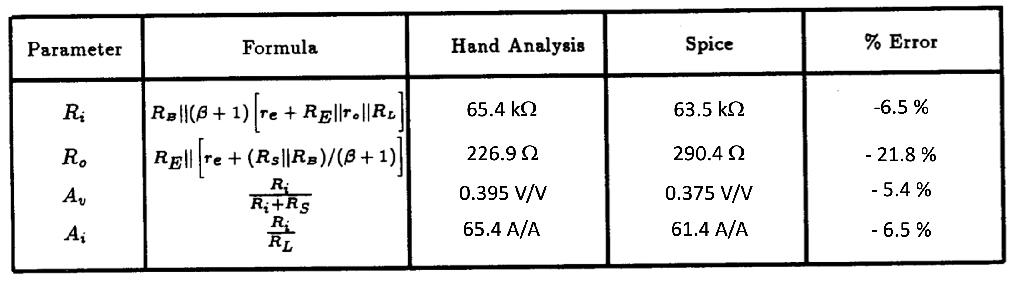
The Common-Collector Amplifier
This same analysis can be repeated for the common-collector (CC) amplifier configuration shown in Fig. 4.24(c). Rather than list much of the same as that seen previously, we simply summarize the results in Table 4.6. As before, the LTSpice results are in good agreement with those obtained with hand analysis.
|
(a)
(b)
Fig. 4.35: A simple transistor switching circuit: (a) schematic, and (b) LTSpice captured circuit schematic with transistor model statement and DC sweep directive included. |
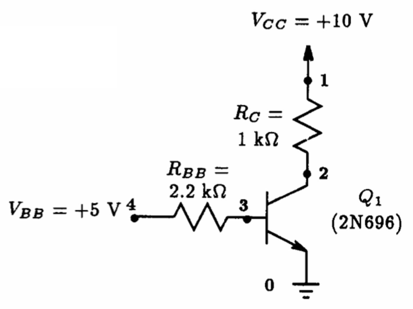
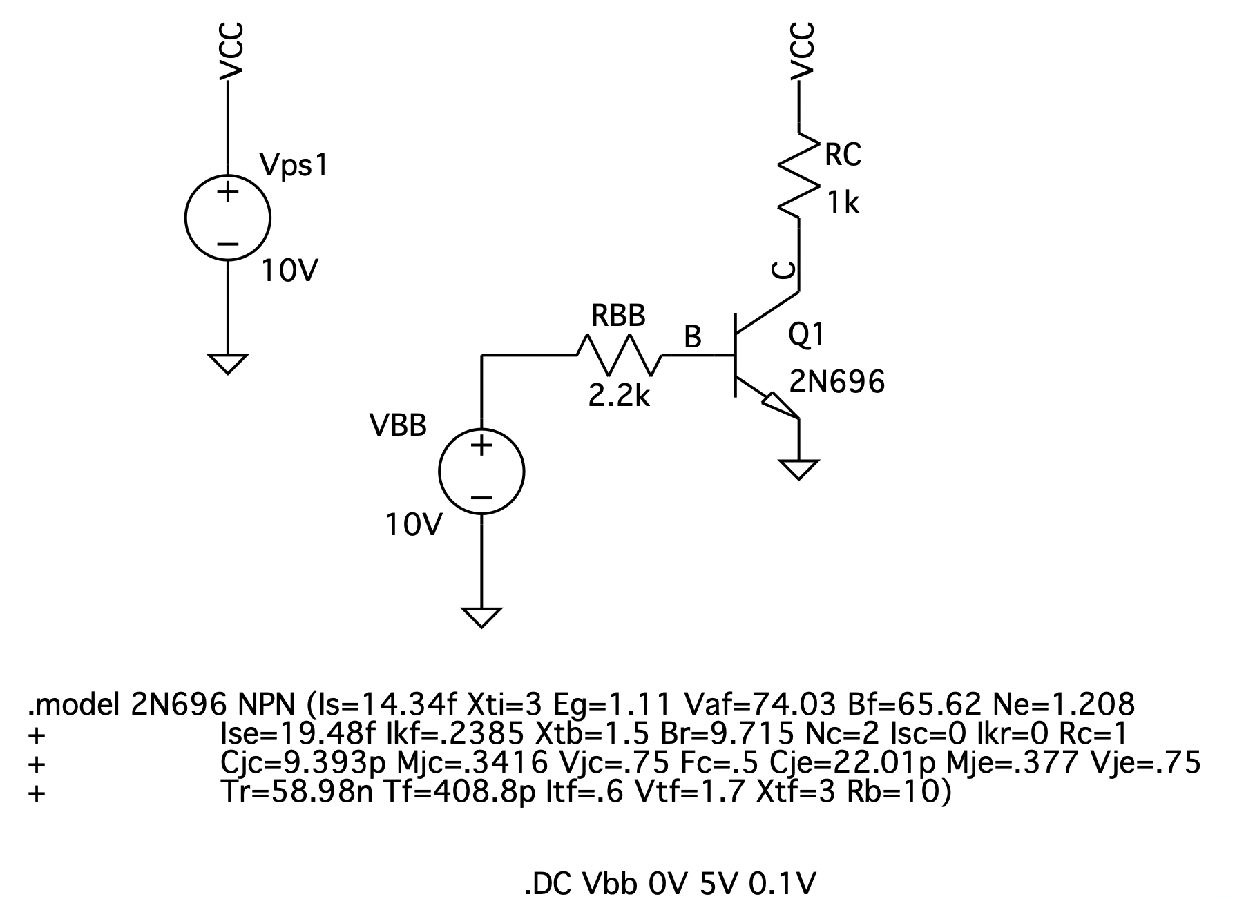
Using The 2N696 NPN Transistor As A Switch * * Circuit Description * * power supplies Vps1 VCC 0 10V * input signal VBB N001 0 10V * transistorized switch Q1 C B 0 0 2N696 RC VCC C 1k RBB B N001 2.2k * transistor model statement for the 2N696 .model Q2N696 NPN (Is=14.34f Xti=3 Eg=1.11 Vaf=74.03 Bf=65.62 Ne=1.208 + Ise=19.48f Ikf=.2385 Xtb=1.5 Br=9.715 Nc=2 Isc=0 Ikr=0 Rc=1 + Cjc=9.393p Mjc=.3416 Vjc=.75 Fc=.5 Cje=22.01p Mje=.377 Vje=.75 + Tr=58.98n Tf=408.8p Itf=.6 Vtf=1.7 Xtf=3 Rb=10) * unused model statements that appear by default of accessing BJT .model NPN NPN .model PNP PNP .lib /Users/roberts/Library/Application Support/LTspice/lib/cmp/standard.bjt * * Analysis Requests * .DC Vbb 0V 5V 0.1V .backanno .end
Fig. 4.36: The LTSpice generated circuit netlist for calculating the overdrive factor associated with the switching circuit shown in Fig. 4.35. The transistor is modeled after the commercial npn transistor 2N696.
|
|
|
|
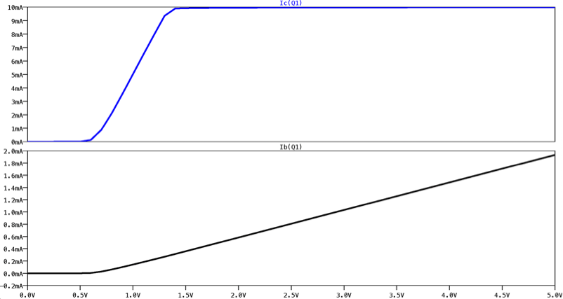
Fig. 4.37: The collector and base current characteristics of the transistor in the circuit of Fig. 4.35 as functions of the base driving voltage VBB. The top curve displays the collector current and the bottom trace displays the base current.
|
4.6 The Transistor as a Switch
As the final example of this chapter, consider the simple transistor switching circuit shown in Fig. 4.35(a). This particular circuit was designed so that transistor Q1 is in saturation with an overdrive factor larger than 10 when the transistor has a minimum beta (β) of 50. With the aid of LTSpice, the overdrive factor of the transistor in this circuit is to be determined when the transistor is assumed to be the commercial 2N696 npn device and the base driving voltage VBB equals 5 V.
The overdrive factor (OD) of a saturated transistor is defined as the ratio of the base current IB divided by the minimum base current that will force the transistor into saturation, denoted as IBsat. Thus,
(4.21)
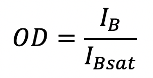
Correspondingly, at the minimum base current condition, the transistor is beginning to conduct a collector current ICsat. Moreover, as the device is driven further into saturation the collector current remains fairly constant at ICsat. Thus, the point at which the collector current begins to saturate denotes the edge of the saturation region. Using LTSpice, the input condition that gives rise to the transistor entering its saturation region in the circuit of Fig. 4.33 will be computed. This can be accomplished by sweeping the base driving voltage VBB between ground and 5 volts and observing both the collector current and the base current of the transistor. From this, we can then determine the base current IBsat. Moreover, at VBB=5 V, we can determine the base current IB and thus the overdrive factor OD for this particular circuit.
The LTSpice captured circuit schematic for the switching circuit shown in Fig. 4.35(a) can be seen in Fig. 4.35(b) and the corresponding LTSpice generated circuit netlist is shown listed in Fig. 4.36. Here a DC sweep analysis is requested that varies the input voltage VBB between 0 and 5 volts in 0.1-volt increments. The BJT model parameters for the 2N696 npn transistor are also included on the schematic, as it was not available in the LTSpice library. This model was downloaded from the internet and included on the schematic using a Spice directive.
The results of the LTSpice analysis are shown plotted in Fig. 4.36. The upper trace displays the transistor collector current IC as a function of the base driving voltage VBB, and the lower trace displays the corresponding base current IB for the same input voltage. Using the cursor feature in waveform viewer we find from the trace of the collector current that it begins to saturate at a current level of 9.79 mA when the base driving voltage VBB exceeds 1.4 V. Correspondingly, from the trace of the transistor base current, we find that at an input voltage VBB of 1.4 V, the base current is 313.6 uA. Hence, IBsat=313.6 uA. Also, we find at an input voltage level of VBB=5 V, the transistor base current IB is 1.932 mA. Therefore, using Eqn. (4.21), we compute the overdrive factor OD for transistor Q1 to be 6.16.
|
|
|
Table 4.3: Key statements for a Monte Carlo circuit analysis. Various random number generator function calls and the .STEP directive to call out different random values.
|
|
|
|
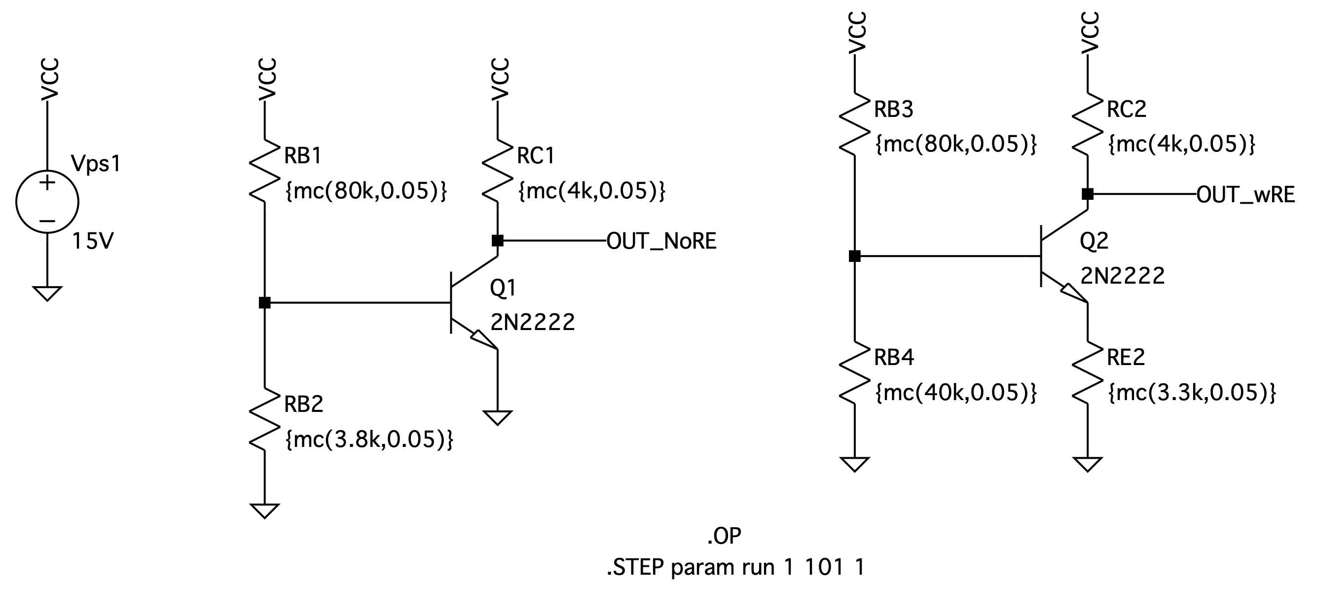
Fig. 4.38: LTSpice circuit capture for comparing the sensitivity of its biasing circuit on the transistor current level. The circuit on the left involves a transistor biasing arrangement without an emitter resistor, whereas the circuit on the right contains an emitter resistor. All resistors are assumed to vary about a nominal value with a uniformly distribution having a ±5% variation. Both circuits operate at a collector voltage of 10 V and the same current level.
|
|
Investigating The Sensitivity Of the Collector Current To Resistor Variations
* * Circuit Description * * power supply Vps1 VCC 0 15V * * amplifier circuit without Re * Q1 OUT_NoRE N002 0 0 2N2222 RB1 VCC N002 {mc(80k,0.05)} RB2 N002 0 {mc(3.8k,0.05)} RC1 VCC OUT_NoRE {mc(4k,0.05)} * * amplifier circuit with Re * Q2 OUT_wRE N001 N003 0 2N2222 RB3 VCC N001 {mc(80k,0.05)} RB4 N001 0 {mc(40k,0.05)} RC2 VCC OUT_wRE {mc(4k,0.05)} RE2 N003 0 {mc(3.3k,0.05)} * transistor model statement for the 2N2222 .lib /Users/roberts/Library/Application Support/LTspice/lib/cmp/standard.bjt * unused model statements that appear by default of accessing BJT .model NPN NPN .model PNP PNP * * Analysis Requests * *.OP .STEP param run 1 101 1 .backanno .end
|
|
Fig. 4.39: The LTSpice generated circuit netlist for the circuit captured in Fig. 4.X for investigating the emitter current variation with ±5% resistor variations.
|
|
|
|
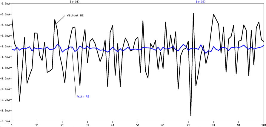
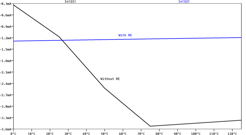
Fig. 4.40: The emitter currents of the amplifier with and without RE. Clearly, the circuit with RE has lower sensitivity to resistor variations than the one with RE included.
|
4.7 DC Bias Sensitivity Analysis Using A Monte Carlo Analysis Approach
Sensitivity to Component Variations
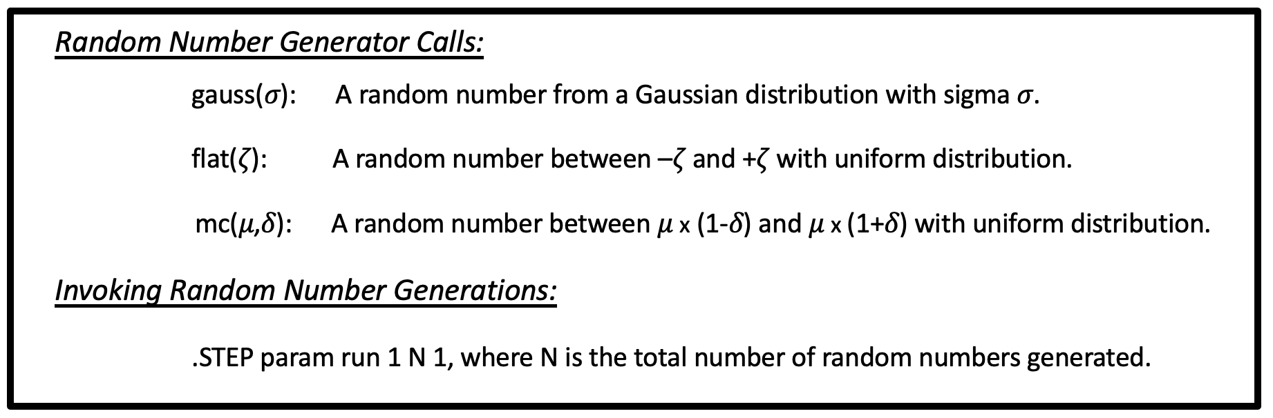
Bias networks are used in transistor amplifier design to establish the proper DC operating point of each transistor. In order to maintain consistent operation, the DC operating point of each transistor must be held constant. This is normally achieved by a bias network that maintains the emitter current of each transistor relatively constant under potential circuit variations, e.g., variations in biasing resistor values, transistor parameters such as beta (β), Early voltage, etc.. Provisions have been made in LTSpice for investigating circuit behavior in the face of component variations through a .STEP directive combined with a set of random number function calls.
The random number generator is invoked by using a specific function call named gauss(𝜎), flat(𝜁) or mc(𝜇,𝜎), depending on the function. In the case of the function, gauss(𝜎), it will generate a random number from a normal or Gaussian distribution that has a mean value of 0 and a sigma set equal to 𝜎. In the case of the flat(𝜁) function call, here a random variable with a uniform distribution from - 𝜁 to 𝜁 will be generated. Finally, the random variable function call mc(𝜇,𝛿) will generate a random variable with a uniform distribution from 𝜇(1-𝛿) to 𝜇(1+𝛿). This is equivalent to saying 𝜇 sets the nominal value of the random variable and 𝛿 is its relative tolerance.
For each step of the .STEP declared iteration, a component or model parameter that is assigned a random variable, will get a new value and the Spice directive such as .OP, .AC or .TRAN will be evaluated using these new component values. On completion of the .STEP directive, the circuit voltage and current variables are available for viewing or printing. If N steps are involved in the .STEP iteration process, then each voltage or current variable will have N values associated with it, thus providing some insight into the effects of component variations. The variable used in the .STEP directive has no physical meaning except that it represent the label assigned that particular iteration. To keep things simple, it is common to refer to each iteration of the analysis the ``run’’ and write the .STEP directive as follows
.STEP param run 1 N 1
Here the parameter run has a start value of 1, an end value of N, and an iteration step size of 1, where N represents the total number of iterations that will be used in random variable analysis. The variable run is a dummy variable but the data that is plotted on completion will be plotted with respect to this value. A summary of these function calls along with the .STEP directive are listed in Table 4.3. The nature of this analysis is referred to as a Monte Carlo analysis for its similarity to the gambling games played at casinos in Monte Carlo, Monaco.
Consider the two BJT amplifiers shown in Fig. 4.38 in the same command window of LTSpice. The transistors are modeled on the widely available commercial transistor 2N2222. The two circuit differ in their biasing arrangement. The circuit on the left biases the npn transistor using three resistors: RB1, RB2 and RC1, whereas the circuit on the right uses four resistors: RB1, RB2, RE2 and RC2. The importance of the emitter resistor RE2 can be seen from a Monte Carlo analysis. This is achieved by assigning all the resistors a random variable using an mc(x,y) function call. The x parameter will take on the nominal resistor value, and the y parameter will be assigned a value of 0.05 to correspond to a ±5% variation. The nominal value of each resistor component can be seen from the schematic in Fig. 4.38. These were chosen to set the emitter currents equal in each circuit. The .STEP command was set for 101 iterations using the statement
.STEP param run 1 101 1
and a dc operating point analysis using .OP was requested. The LTSpice generated circuit netlist is shown in Fig. 4.39.
On completion, the emitter currents of the two circuits can be seen plotted in Fig. 4.40. As is clearly evident, the circuit with an emitter resistor experiences much smaller variation than the circuit that does not use one. Approximately, an order of magnitude less variation. This is a result of the localized feedback provided by the emitter resistor.
|
|
|
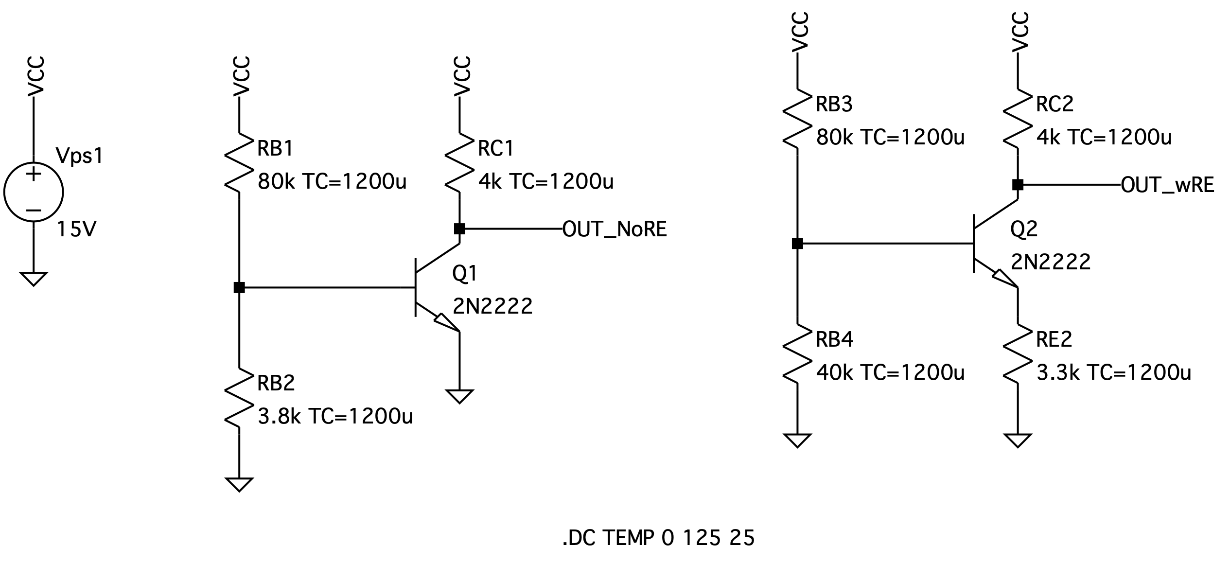
Fig. 4.41: LTSpice circuit capture for comparing the temperature dependence of its biasing circuit on the transistor current level. The circuit on the left involves a transistor biasing arrangement without an emitter resistor, whereas the circuit on the right contains an emitter resistor. The DC operation of the circuit is evaluated over a temperature range from 0 degree-C to 125 degree-C in 25 degree-C steps. All resistors are assumed to depend on temperature with a TC=1200u ppm/°C.
|
|
Investigating Emitter Current Dependence On Temperature
* * Circuit Description * * power supply Vps1 VCC 0 15V * * amplifier circuit without Re * Q1 OUT_NoRE N002 0 0 2N2222 RB1 VCC N002 80k TC=1200u RB2 N002 0 3.8k TC=1200u RC1 VCC OUT_NoRE 4k TC=1200u * * amplifier circuit with Re * Q2 OUT_wRE N001 N003 0 2N2222 RB3 VCC N001 80k TC=1200u RB4 N001 0 40k TC=1200u RE2 N003 0 3.3k TC=1200u RC2 VCC OUT_wRE 4k TC=1200u * transistor model statement for the 2N2222 .lib /Users/roberts/Library/Application Support/LTspice/lib/cmp/standard.bjt * unused model statements that appear by default of accessing BJT .model NPN NPN .model PNP PNP * * Analysis Requests * .DC TEMP 0 125 25 .bakanno .end |
|
Fig. 4.42: Temperature variation of the emitter currents in the two amplifier circuits shown in Fig. 4.41.
|
|
|
Fig. 4.43: The temperature dependency of the emitter currents of the amplifier with and without RE. Clearly, the circuit with RE has lower temperature sensitivity to resistor variations than the one with RE included. |
Sensitivity to Temperature Variations
To investigate the bias stability of the two amplifiers seen in Fig. 4.38 subject to temperature changes requires a different approach than that just seen using a Monte Carlo analysis. For such cases, we make use of an extension to the DC sweep command which will allow the user to sweep the temperature of the circuit over a specified range while repeatedly performing a DC analysis. The syntax of this command is identical to any other DC sweep command with the keyword TEMP replacing the field marked by source_name. The range of temperature values is specified in exactly the same way as for a voltage or current source. For this particular example, we will monitor the emitter current over a temperature range beginning at 0°C and ending at 125°C in steps of 25°C. The exact syntax of this DC sweep command can be seen in the LTSpice schematic capture window shown in Fig. 4.41.
The built-in model for the BJT accounts for variations in temperature. The same cannot be said for the resistors. In order to account for changes in resistance due to temperature variations, one must indicate the temperature dependency using a array of temperature coefficients TC1, TC2 , TC3 , …. These coefficients are incorporated into the resistance formula according to the following polynomial equation,
(4.11)
![]()
For our purposes here, we shall consider only the linear dependence of resistance on temperature, and therefore, consider higher order TC terms equal to zero, i.e., TC2=0, TC3=0, … We shall assume for this example, that TC1 = 1200 ppm/°C, where ppm denotes parts-per-million or a multiplication factor of 10-6. To specify the dependence of a resistor on temperature in LTSpice, one simply appends to the resistor statement after the resistor value is entered, TC= TC1, TC2, TC3, … In this particular case, we will write TC=1200u. All this can be seen from in the LTSpice captured circuit and the corresponding circuit netlist shown in Fig. 4.42.
The results of the emitter current dependence on temperature are summarized in Fig. 4.43 for the amplifier with and without emitter resistance. Once again, the amplifier without an emitter resistor is strongly dependent on temperature, whereas the other is not.
4.8 Chapter Summary
· A BJT is described to LTSpice using an element statement and a model statement.
· The element statement describes how the base, collector, and emitter of a transistor are connected to the rest of the network.
· The model statement contains a list of parameters describing the terminal characteristics of a BJT using the built-in model of LTSpice.
· There are 40 parameters associated with the built-in LTSpice model of the BJT. (We discussed only 6 of them, the remainder are described in the Appendix).
· A specific transistor mode of operation is deduced from the DC voltages that appears across its emitter-base junction and collector-base junction. This information can be found in the Spice Error Log file as a result of an operating point (.OP) analysis.
· When an operating point (.OP) calculation is included in the LTSpice command window/schematic, a list of operating point information for each transistor is obtained. This information contains DC bias conditions for the transistor and the parameters associated with its small-signal model.
· Models of many commercial bipolar transistors are available from various semiconductor manufacturers. A library of transistor models for various commercial transistors are available with the LTSpice program.
· LTSpice can be used to generate families of i-v curves for transistors, just like the laboratory curve-tracer instrument.
· If the effect of decoupling and by-pass capacitors is to be ignored then their values should be selected to be very large during the simulation (generally, a good value is 1 F in LTSPice). One must be careful not to include the F in the device value, as the F will be interpreted to be a multiplier of 10-15.
· LTSpice can perform Monte Carlo simulation; this can be used to investigate the circuit robustness to manufacturing issues.
· LTSpice can be used to investigate a circuit temperature dependence.
4.9 LTSpice Tips
· Random number generators are used to model a component whose value is treated as a random variable. There are three types of random number generator available in LTSpice: zero-mean value Gaussian distribution, zero-mean value uniform distribution, and a non-zero mean-value uniform distribution.
+ A zero-mean value Gaussian distributed random variable with standard deviation 𝜎 is called using the function gauss(𝜎).
+ A zero-mean value uniform distributed random variable from -𝜁 to 𝜁 is called using the function flat(𝜁).
+ A component with value 𝜇 that is uniformly distributed from 𝜇*(1-𝛿) to 𝜇*(1+𝛿) is called using the function mc(𝜇,𝜎).
+ All random variable calls must be placed inside brackets, { }.
· To invoke the selection of a new random component for a Spice analysis involving N trials, the following .STEP directive is used:
.STEP PARAM run 1 N 1
where run is just a dummy variable representing the sample iteration.
4.10 Bibliography
L. W. Nagel, SPICE2 - A computer program to simulate semiconductor circuits, Memorandum no. ERL-M520, May 1975, Electronic Research Laboratory, University of California, Berkeley.
N. R. Malik, Determining Spice parameter values for BJT's, IEEE Transaction on Education, vol. 33, No. 4, pp. 366-368, Nov. 1990.
4.11 Problems
4.1. Consider the case of a transistor whose base is connected to ground, the collector is connected to a 10 V dc source through a 1 k-ohm resistor, and a 5-mA current source is connected to the emitter with the polarity so that current is drawn out of the emitter terminal. If βF=100 and IS =10-14 A, find the voltages at the emitter and the collector using Spice. Further, determine the base current.
4.2. Using the Spice model parameters for the commercial 2N2222A npn BJT given in Section 4.5, determine its leakage current ICBO at room temperature (i.e., 27°C). If the temperature of the device is raised to 75°C, what is the new ICBO? Hint: Connect the base to ground, the collector to +5 V, and do not connect the emitter terminal. The current supplied by the +5 V voltage source is ICBO.
4.3. Consider a pnp transistor having IS=10-13 A and βF=40. If the emitter is connected to ground, the base is connected to a current source that pulls out of the base terminal a current of 10 𝜇A, and the collector is connected to a negative supply of -10 V via a 10 kΩ resistor, find the base voltage, the collector voltage, and the emitter current using the operating point (.OP) command of Spice.
4.4. Using Spice as a curve tracer, plot the iC - vCE characteristics of an npn transistor having IS=10-15 A and VA=100 V. Provide curves for vBE=0.65, 0.70, 0.72, 0.73 and 0.74 volts. Show the characteristics for vCE up to 15 V.
4.5. For a BJT having an Early voltage of 200 V, what is its output resistance at 1 mA as calculated by Spice? at 100 𝜇A?
4.6. The transistor in the circuit of Fig. P4.6 has a very high βF (assume at least 106 in the Spice file). The other parameters of the transistor Spice model can assume default values. Find VE and VC for VB equal to (a) +3 V, (b) +1 V, and (c) 0 V. What is the transistor mode of operation in each case?
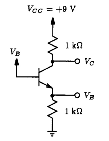
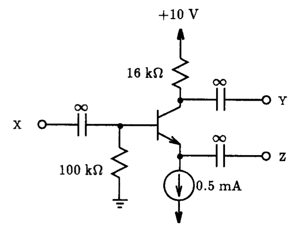
Fig. P4.6 Fig. P4.9
4.7. For the circuit in Fig. P4.6, with the aid of Spice and VB set equal to +2 V, find all node voltages for (a) βF very high (>106), and (b) βF=99.
4.8. In the circuit of Fig. 4.16, the input signal vi is described by 0.004 sin(wt) volts and the transistor is assumed modeled after the 2N2222A type. In addition, VBB is reduced from 3 V to 1 V. Using Spice, plot the base and collector current of Q1 as a function of time for at least one period of the input signal. Likewise, plot the collector voltage of Q1. What is the voltage gain of this amplifier?
4.9. The transistor shown in the circuit of Fig. P4.9 has βF=100 and VA=80 V. Use Spice to answer the following questions, but also compare your results with those obtained through a hand analysis:
a) Find the dc voltages at the base, emitter, and collector using Spice. Represent the infinite-valued capacitors with a very large, but finite, value.
b) Find gm, rp, and ro.
c) If terminal Z is connected to ground, X to signal source Vs having a 10 kΩ source resistance, what is the voltage gain vy/vs. Since the capacitor connected to node Y is left floating, either connected a large load to node Y or remove this capacitor and take the measurement directly from the collector of the transistor.
d) If terminal X is connected to ground, Z to an input signal source vs having a 200-Ω source resistance, and Y to a load resistance of 10 kΩ, find the voltage gain vy / vs.
e) If terminal Y is connected to ground, X to an input signal source vs having a 100 kΩ source resistance, and Z to a load resistance of 1 kΩ, find the voltage gain vz / vs.
4.10. With the aid of Spice, verify the design of a version of the circuit in Fig. 4.23 that uses ±9.5 V supplies for operation at 10 mA (for high βF), such that the total variation in IE is less than 5% for βF as low as 50. To obtain the highest possible voltage gain, select the largest possible value for RC; however, you must ensure that VCE is never less than 2 V.
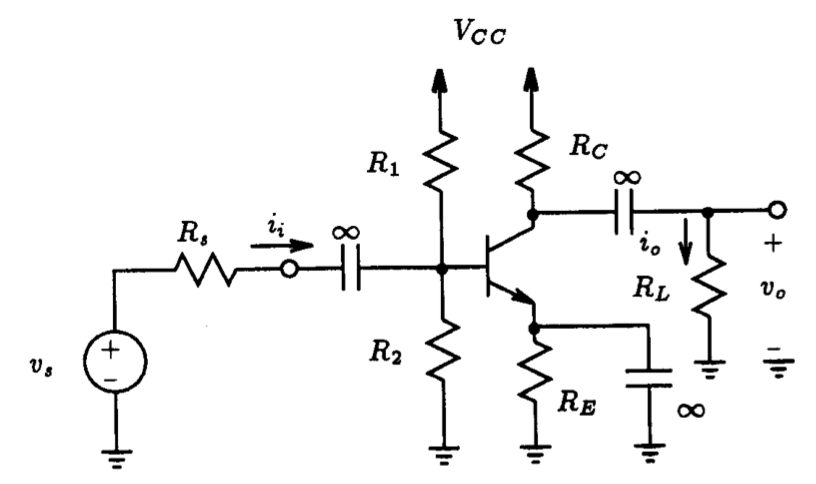
Fig. P4.11
4.11. For the common-emitter amplifier shown in Fig. P4.11, let VCC=9 V, R1=27 kΩ, R2=15 kΩ, RE=1.2 kΩ, and RC=2.2 kΩ. The transistor has βF=100 and VA=100 V. Using Spice, calculate the dc bias current IE. If the amplifier operates between a source for which Rs=10 kΩ and a load of 2 kΩ, determine the values of Ri, Gm, Ro, Av, and Ai.
4.12. Repeat Problem 4.11 with the transistor modeled after the commercial transistor 2N696. Use the Spice parameters for the 2N696 provided in Section 4.6.
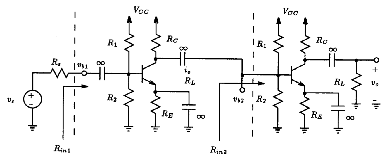
Fig. P4.13
4.13. The amplifier of Fig. P4.13 consists of two identical common-emitter amplifiers connected in cascade.
a) For VCC=15 V, R1=100 kΩ, R2=47 kΩ, RE=3.9 kΩ, RC=6.8 kΩ, and βF=100, determine the dc collector current and collector voltage of each transistor using Spice. The amount of data that must be typed into the computer is reduced if a subcircuit is created for one of the stages and used twice to form the overall amplifier.
b) Find Rin1 and vb1/vs for Rs=5 kΩ.
c) Find Rin2 and vb2/vb1 for Rs=5 kΩ.
d) For RL=2 k-ohm, find vo/vs.
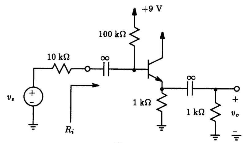
Fig. P4.14
4.14. For the emitter-follower circuit shown in Fig. P4.14 the BJT used is specified to have βF values in the range of 20 to 200. For the two extreme values of B find:
a) IE, VE and VB.
b) the input resistance Ri.
c) the voltage gain vo/vs.
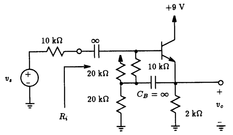
Fig. P4.15
4.15. For the bootstrapped follower circuit shown in Fig. P4.15 where the transistor is assumed to be of the 2N2222A type, compare the input and output resistance, and the voltage gain vo/vs, with and without the bootstrapping capacitor CB in place.
4.16. One small-signal BJT model parameter that is used in the small-signal calculations of Spice but is not sent to the Spice output file when an .OP command is specified is ru. Devise a simple circuit arrangement for calculating this small-signal resistance with Spice.