Chapter 5
Field-Effect Transistors (FETs)
Gordon W. Roberts
Department of Electrical & Computer Engineering, McGill University
In this chapter we shall show how LTSpice is used to simulate circuits containing field-effect transistors (FETs). LTSpice has built-in models for two of the three FET types considered here, metal-oxide-semiconductor FETs (MOSFETs) and junction FETs (JFETs). In the case of metal-semiconductor FETs (MESFETs), we shall carry out our circuit simulations using the built-in model of LTSpice. Various circuit examples involving the three types of FETs will be given.
5.1 Describing MOSFETs To Spice
MOSFETs are described to Spice using two statements; one statement describes the nature of the FET and its connections to the rest of the circuit, and the other specifies the values of the parameters of the built-in FET model. The following outlines the syntax of these two statements, including some details on the built-in ``Level 1'' MOSFET model of Spice.
|
Fig. 5.1: Spice element description for the NMOS and PMOS MOSFETs. Also listed is the general form of the associated MOSFET model statement. A partial listing of the parameter values applicable to either the NMOS or PMOS MOSFET is given in Table 5.1. Enhancement or depletion mode of operation is determined by the values assigned to these parameters.
|
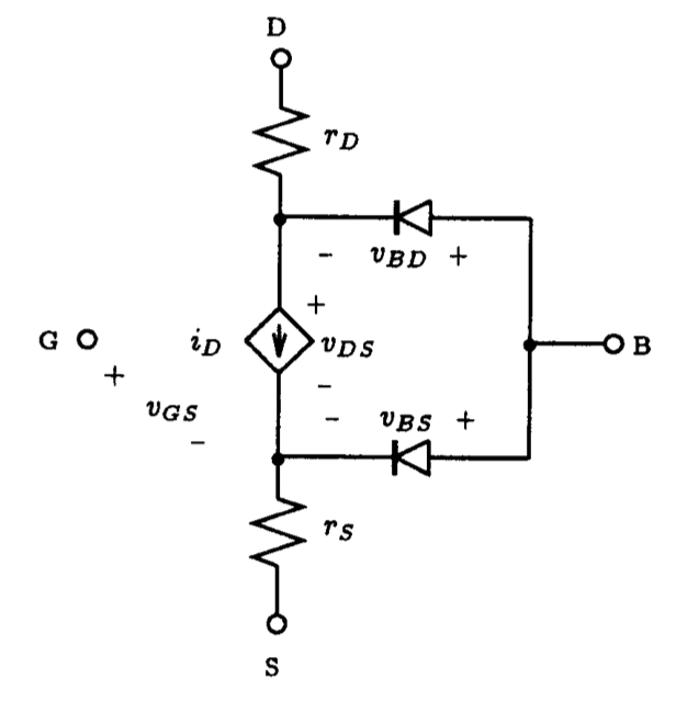
Fig. 5.2: The general form of the Spice large-signal model for an n-channel MOSFET under static conditions.
|

|
Table. 5.1: A partial listing of the Spice parameters for the LEVEL 1 MOSFET model.
|
5.1.1 MOSFET Element Description
The presence of a MOSFET in a circuit is described to Spice through the Spice input file using an element statement beginning with the letter M. If more than one MOSFET exists in a circuit, then a unique name must be attached to M to uniquely identify each transistor. This is then followed by a list of the nodes that the drain, gate, source, and substrate (body) of the MOSFET are connected to. Subsequently, on the same line, the name of the model that will be used to characterize a particular MOSFET is given. The name of this model must correspond to the name given on a model statement containing the parameter values that characterize this MOSFET to Spice. Finally, the length and width of the MOSFET are given. For quick reference, we depict in Fig. 5.1 the syntax for the Spice statement describing the MOSFET. Also listed is the syntax for the model statement (.MODEL) that must be present in any Spice input file that makes reference to the built-in MOSFET model of Spice. This statement specifies the terminal characteristics of the MOSFET by defining the values of particular parameters in the MOSFET model. Parameters of the model not specified are assigned default values by Spice. We shall briefly discuss the model statement next.
5.1.2 MOSFET Model Description
As is evident from Fig. 5.1, the model statement for either the NMOS or PMOS transistor begins with the keyword .MODEL and is followed by the name of the model used by a MOSFET element statement, the nature of the MOSFET (i.e., NMOS or PMOS), and a list giving the values of the model parameters (enclosed between brackets). The number of parameters associated with the Spice model of the MOSFET is large and their meaning complicated; besides, Spice has more than one large-signal model for the MOSFET. These are classified according to their levels of sophistication: Level 1, 2 and 3. The simplest MOSFET model being that described in Level 1. For the most part, MOSFET behavior described in Chapter 5 of Sedra and Smith is based on the Level 1 MOSFET model. The other two models are more complicated, and their mathematical description will not be discussed here. Rather, we shall just mention their important differences. The Level 2 MOSFET model is a more complex version of the LEVEL 1 model which includes extensive second-order effects, largely dependent on the geometry of the MOSFET. The Level 3 MOSFET model of Spice is a semi-empirical model (having some model parameters that are not necessarily physically based), especially suited to short-channel MOSFETs (i.e., L £ 5 𝜇m). For more details on these models, interested readers can consult reference [Vladimirescu, 1980].
Also, an advanced VLSI textbook by Geiger, Allen and Strader [Geiger, Allen and Strader, 1990] provides a good review of the three MOSFET models of Spice.
The general form of the DC Spice model for an n-channel MOSFET is illustrated schematically in Fig. 5.2. The bulk resistance of both the drain and source regions of the MOSFET are lumped into two linear resistances rD and rS, respectively. The DC characteristic of the intrinsic MOSFET is determined by the nonlinear dependent current source iD, and the two diodes represent the two substrate junctions that define the channel region. A similar model exists for the p-channel device; the direction of the diodes, the current source and the polarities of the terminal voltages are all reversed. The mathematical relationship that describes the DC behavior of the dependent current source varies depending on which level of model is used. For the LEVEL 1 MOSFET model, the expression for drain current iD, assuming that the drain is at a higher potential than the source, is described by the following:
where the device constant K is related to process parameters and device geometry according to
(5.2)
and the threshold voltage Vt is given by
(5.3)
Here we see that the drain current equations are determined by the eight parameters: W, L, 𝜇, COX, Vt0, lambda, g and 2ff. Both W and L define the dimensions of the device. These two parameters are usually specified on the element statement of the MOSFET, although, if none is specified, Spice will assume that both W and L are 100 𝜇m. Parameters 𝜇 and COX are process-related parameters that are multiplied together to form the process transconductance coefficient kp. It is kp that is usually specified in the parameter list of the model statement. The parameter Vt0 is the zero-bias threshold voltage. Vt0 is positive for enhancement-mode n-channel MOSFETs and depletion-mode p-channel MOSFETs. But Vt0 is negative for depletion-mode n-channel MOSFETs and enhancement-mode p-channel MOSFETs. The parameter 𝜆 is the channel-length modulation parameter and represents the influence that drain-source voltage has on the drain current iD when the device is in saturation. In Spice, the sign of this parameter is always positive, regardless of the nature of the device type. The last two parameters, 𝛾 and 2𝜙f, are the body-effect parameter and the surface potential, respectively.
A partial listing of the parameters associated with the Spice MOSFET model under static conditions is given in Table 5.1. Also listed are default values which a parameter assumes if a value is not specified for it on the .MODEL statement. To specify a parameter value one simply writes, for example: level=1, kp=20𝜇, Vto=1V, etc.
|
(a)
(b)
Fig. 5.3: A MOSFET circuit example: (a) circuit schematic, and (b) entered into LTSpice using schematic capture.
|
Simple Enhancement-Mode MOSFET Circuit
** Circuit Description ** * dc supplies Vps1 VDD 0 5V Vps2 0 VSS 5V * MOSFET circuit M1 D 0 S S nmos_enhancement_mosfet L=10u W=400u RD VDD D 10k RS S VSS 5k * mosfet model statement (by default, level 1) .model nmos_enhancement_mosfet nmos (kp=20u Vto=+2V lambda=0) * unused model statement calls .model NMOS NMOS .model PMOS PMOS .lib /Users/roberts/Library/Application Support/LTspice/lib/cmp/standard.mos * * Analysis Requests * * calculate DC bias point .OP .backanno .end
Fig. 5.4: LTSpice generated circuit netlist for computing the DC operating point of the MOSFET circuit shown in Fig. 5.3.
|
|
|
|

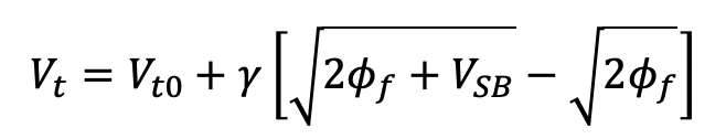
5.1.3 An Enhancement-Mode N-Channel MOSFET Circuit
In the following we shall calculate the DC conditions of a circuit containing a FET using LTSpice. Both the DC node voltages of the circuit and the DC operating point information of the FET will be determined.
Consider the circuit shown in Fig. 5.3. Here we would like to confirm that the FET is indeed biased at a current level of 0.4 mA and that the voltage appearing at the drain is +1 V, as determined by a hand analysis. The NMOS transistor is assumed to have Vt=2 V, 𝜇nCOX= 20 𝜇A/V2, L=10 𝜇m, and W=400 𝜇m. Furthermore, the channel-length modulation effect is assumed zero (i.e., lambda=0). Assuming a level 1 MOSFET model, we can create the following LTSpice model statement for this FET using the above information as:
.model nmos_enhancement_mosfet nmos (kp=20u Vto=+2V lambda=0)
Here, we have labeled the name of this model as: nmos_enhancement_mosfet. The meaning behind this name should be obvious. Constructing the circuit as per the schematic diagram of Fig. 5.3(a) by accessing the appropriate components using the Component list of the schematic capture tool, including the NMOS transistor results in the circuit schematic shown in Fig. 5.3(b). In this case, the MOSFET is selected to be the three terminal type where the source and body terminals are assumed connected together. One could have just as easily selected the four terminal MOSFET and added a wire to connect the source and body together. The attributes of the MOSFET are modified so that it refers to the nmos_enhancement_mosfet model, and, in addition, the length and width of the transistor is included on the same statement as the model name, as illustrated in Fig. 5.3(b). Without such information, the transistor aspect ratio will take on default values. The NMOS model statement is also included in the schematic command window. A dc operating point analysis is requested using the .OP command. The corresponding LTSpice generated circuit netlist can be seen listed in Fig. 5.4.
The results of the dc analysis result in the following operating point information:
|
Semiconductor Device Operating Points:
--- MOSFET Transistors --- Name: m1 Model: nmos_enhancement_mosfet Id: 4.00e-04 Vgs: 3.00e+00 Vds: 4.00e+00 Vbs: 0.00e+00 Vth: 2.00e+00 Vdsat: 1.00e+00
Operating Bias Point Solution:
V(vdd) 5 voltage V(d) 1 voltage V(s) -3 voltage V(vss) -5 voltage Id(M1) 0.0004 device_current Ig(M1) 0 device_current Ib(M1) -4.01e-12 device_current Is(M1) -0.0004 device_current I(Rs) 0.0004 device_current I(Rd) 0.0004 device_current I(Vps2) -0.0004 device_current I(Vps1) -0.0004 device_current
|
As expected, these results confirm that the FET is biased at the intended current level of 0.4 mA, and also that the drain of the FET is at the correct voltage level of +1 V. As a further note, we see from the above results that M1 is biased in its saturation region because vDS > VDS,SAT where LTSpice uses the notation Vdssat = VGS - Vt.
|
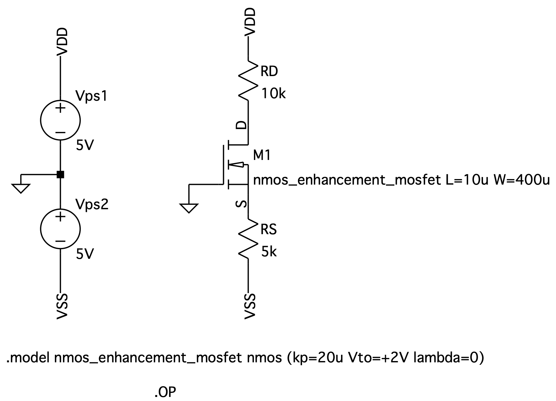
Fig. 5.5: LTSpice curve-tracer arrangement for calculating the i - v characteristics of a MOSFET. The iD - vDS characteristic of the MOSFET is obtained by sweeping vDS through a range of voltages while keeping VGS constant at some value. Here the channel-length modulation factor (lambda) is varied from 0 to 0.05 V-1 in 0.01 V-1 increments.
|
Enhancement-Mode N-Channel MOSFET Id - Vds Characteristics
** Circuit Description ** * dc supplies VDS C 0 0V VGS N001 0 3V * MOSFET circuit M1 C N001 0 0 nmos_enhancement_mosfet L=10u W=400u RD VDD D 10k RS S VSS 5k * mosfet model statement (by default, level 1) .model nmos_enhancement_mosfet nmos (kp=20u Vto=+2V lambda={lambda_variable}) * unused model statement calls .model NMOS NMOS .model PMOS PMOS .lib /Users/roberts/Library/Application Support/LTspice/lib/cmp/standard.mos * * Analysis Requests * * calculate DC bias point .DC VDS 0V 10V 100mV .STEP param lambda_variable 0 0.05 0.01; * vary lambda_variable from 0 to 0.05 in increments of 0.01 .backanno .end
Fig. 5.6: LTSpice generated circuit netlist for computing the the iD - vDS characteristic of a MOSFET with device parameters: Vt=+2 V, un COX= 20 uA/V2, L=10 um, and W=400 um for the circuit shown in Fig. 5.5. The gate-source voltage VGS is set equal to +3 V and the drain-source voltage is swept between 0 and +10 V in 100 mV increments using the .DC sweep command. In addition, the channel-length modulation factor (lambda) is varied from 0 top 0.05 V-1 in 0.01 V-1 increments using the .STEP directive.
|
|
|
|
Fig. 5.7: Comparing the iD - vDS characteristics of a MOSFET with a channel-length modulation factor (lambda) that varies from 0 to 0.05 V-1 in 0.01 V-1 increments. The gate-source voltage is held constant at +3 V.
|

5.1.4 Observing the MOSFET Current - Voltage Characteristics
The iD - vDS characteristics of a MOSFET are easily obtained by sweeping the drain-to-source voltage through a range of DC voltages, all the meanwhile, the gate-to-source voltage is held constant at some voltage value. The drain current of the MOSFET is then monitored and plotted against the drain-source voltage. To demonstrate how one performs this operation on a MOSFET using LTSpice, consider the circuit shown in Fig. 5.5. Here two independent voltage sources, VGS and VDS, will be used to establish the different bias conditions on the enhancement-mode n-channel MOSFET whose source and body are connected together. It is assumed that the MOSFET has the same geometry and device parameters that were previously mentioned in the last subsection. Repeating them here, the NMOS transistor is characterized by Vt=+2 V, 𝜇nCOX= 20 𝜇A/V2, L=10 𝜇m, and W=400 𝜇m. The channel-length modulation factor (lambda) will be assumed to vary from 0 to 0.05 V-1 in 0.01 V-1 increments. In this way, the effects of channel-length modulation can be seen quite clearly. Let us consider setting VGS=+3 V and sweep VDS from 0 V to +10 V in steps of 100 mV. In this way, the MOSFET will be taken through both its triode and saturation regions of operation. The resulting drain current is then monitored by observing the current supplied by voltage source VDS. To achieve a variable transistor model, the .STEP directive will be used in conjunction with a variable written for lambda in the model statement. Specifically, the following two statements would be used:
.model nmos_enhancement_mosfet nmos (kp=20u Vto=+2V lambda={lambda_variable})
.STEP param lambda_variable 0 0.05 0.01; * vary lambda_variable from 0 to 0.05 in increments of 0.01
The schematic captured by LTSpice is shown in Fig. 5.5 and the corresponding circuit netlist is listed in Fig. 5.6. The results of this analysis are shown plotted in Fig. 5.7. For drain-source voltages less than VDS,SAT, (VDS,SAT=VGS-Vt=+1 V), the MOSFET is in its triode region regardless of the lambda value. For drain-source voltages above +1 V, the MOSFET current increases linearity with increasing VDS. The higher the lambda value the higher the slope of the curve in this region. Say, for example, lambda = 0.05 V-1, then one can see that the output current increases with increasing drain-source voltage at a rate of 20.314 𝜇A/V. Thus, the corresponding incremental drain-source resistance is 49.23 kΩ. It is re-assuring that this increment resistance agrees quite closely with the value estimated by hand analysis; e.g., for a drain current of approximately 400 𝜇A, ro which is given by 1/(𝜆 ID), is estimated to be 50 kΩ. For the other curves corresponding to lambda values less than 0.05 V-1, the incremental drain-source resistance would increase with decreasing lambda.
|
|
|
Fig. 5.8: Comparing the iD - VGS characteristics of a MOSFET with a channel-length modulation factor from 0 to 0.05 V-1 in increments of 0.01 V-1. The drain-source voltage is held constant at +5 V and the gate-source voltage varied from 0 to 10 V.
|

Another current - voltage characteristic that is used to describe the behavior of a MOSFET is: iD versus VGS. The circuit arrangement illustrated in Fig. 5.5 can also be used to obtain this current - voltage behavior. Instead of varying the drain-source voltage, this voltage is held constant and the gate-source voltage of the MOSFET is swept over a desired range for different lambda values. To demonstrate this, consider setting VDS to +5 V and sweeping VGS from 0 V to +5 V in increments of 100 mV. The Spice directive would be re-written as
.DC VGS 0V 10V 100mV
The results of this analyses are shown in Fig. 5.8. Here we have plotted the iD - VGS curves for the six values of lambda. As is evident, the presence of a nonzero lambda gives rise to a vertical shift in drain current. One interpretation of this is that for a given gate-source voltage, a MOSFET with non-zero channel-length modulation will draw more current from a circuit than one with zero channel-length modulation.
5.2 LTSpice Analysis of MOSFET Circuits At DC
MOSFETs are classified as n-channel or p-channel devices depending on the material used to form the channel. In addition, these devices are classified according to their mode of operation as enhancement or depletion type devices. As a result, the model statement characterizing these different FETs have subtle differences. In the following we shall highlight these differences as we analyze the DC operating point of several simple MOSFET circuits. Our results will be compared with those derived by hand analysis.
|
Fig. 5.9: A PMOS transistor circuit with DC biasing. LTSpice is used to calculate the DC operating point of this circuit.
|
A Simple Enhancement-Mode PMOS Circuit (Rd=6k) * * Circuit Description * * dc supplies Vps1 S 0 5V * MOSFET circuit M1 D N001 S S pmos_enhancement_mosfet L=10u W=10u RD D 0 6k RG1 S N001 2Meg RG2 N001 0 3Meg * mosfet model statement (by default, level 1) .model pmos_enhancement_mosfet pmos (kp=1m Vto=-1V lambda=0) * unused model related statements .model NMOS NMOS .model PMOS PMOS .lib /Users/roberts/Library/Application Support/LTspice/lib/cmp/standard.mos * * Analysis Requests * * calculate DC bias point .OP .backanno .end
Fig. 5.10: LTSpice generated circuit netlist for calculating the DC operating point of the p-channel MOSFET circuit shown in Fig. 5.19.
|
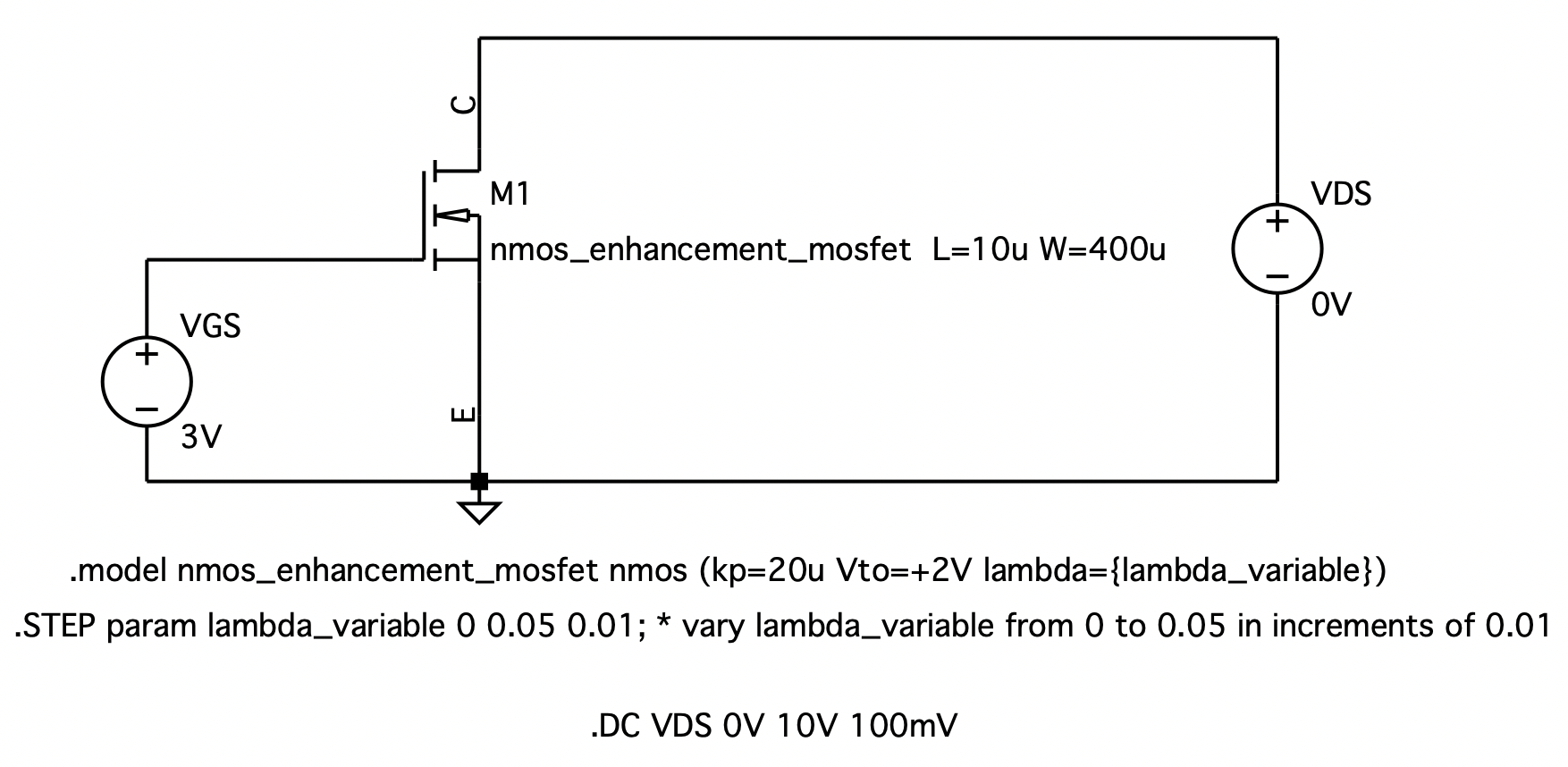
5.2.1 An Enhancement-Mode P-Channel MOSFET Circuit
Consider the LTSpice circuit schematic shown in Fig. 5.9. Here we have a single transistor circuit containing a p-channel enhancement-mode MOSFET with L=10 𝜇m and W=10 𝜇m. The resistors have been chosen such that the FET is biased in its saturation region, has a bias current of 0.5 mA, and a drain voltage of +3 V. It is also assumed that the MOSFET has a threshold voltage of -1 V, a process transconductance parameter 𝜇pCOX equal to 1 mA/V2 and does not exhibit any channel-length modulation effect (i.e., lambda=0). The model statement describing the characteristics of the p-channel MOSFET would appear as follows:
.model pmos_enhancement_mosfet pmos (kp=1m Vto=-1V lambda=0)
Here we have declared the MOSFET to be a PMOS device, and by assigning a negative threshold voltage, we are indicating to Spice that this particular PMOS device is of the enhancement-mode. Finally, a DC operating point analysis directive is requested using the .OP command. The LTSpice generated circuit netlist for this particular example is listed in Fig. 5.10.
Executing the LTSpice analysis results in the following DC operating point information:
|
Semiconductor Device Operating Points:
--- MOSFET Transistors --- Name: m1 Model: pmos_enhancement_mosfet Id: -5.00e-04 Vgs: -2.00e+00 Vds: -2.00e+00 Vbs: 0.00e+00 Vth: -1.00e+00 Vdsat: -1.00e+00
Operating Bias Point Solution:
V(s) 5 voltage V(d) 3 voltage V(n001) 3 voltage Id(M1) -0.0005 device_current Ig(M1) -0 device_current Ib(M1) 2.01e-12 device_current Is(M1) 0.0005 device_current I(Rg1) 1e-06 device_current I(Rg2) 1e-06 device_current I(Rd) 0.0005 device_current I(Vps1) -0.000501 device_current
|
As is evident from above, the p-channel MOSFET is biased at a current level of 0.5 mA and that its drain is set at +3 V. The sign of ID is negative because of the convention adopted by Spice; positive drain current flows into the drain terminal of a FET regardless of the device type. We also know that the device is biased in its saturation region because vDS < VDS,SAT. It is interesting to note that if we alter the value of RD from 6 kΩ to 8 kΩ, and re-run the LTSpice analysis, then we find that M1 is biased on the edge of saturation (i.e., vDS =VDS,SAT), as shown below:
|
Semiconductor Device Operating Points:
--- MOSFET Transistors --- Name: m1 Model: pmos_enhancement_mosfet Id: -5.00e-04 Vgs: -2.00e+00 Vds: -1.00e+00 Vbs: 0.00e+00 Vth: -1.00e+00 Vdsat: -1.00e+00
Operating Bias Point Solution:
V(s) 5 voltage V(d) 4 voltage V(n001) 3 voltage Id(M1) -0.0005 device_current Ig(M1) -0 device_current Ib(M1) 1.01e-12 device_current Is(M1) 0.0005 device_current I(Rg1) 1e-06 device_current I(Rg2) 1e-06 device_current I(Rd) 0.0005 device_current I(Vps1) -0.000501 device_current
|
Any increase in RD above 8 kW will certainly cause M1 to move out of the saturation region and into the triode region.
|
Fig. 5.11: A depletion-mode p-channel MOSEFT circuit.
|
A Depletion-Mode PMOS Transistor Circuit * * Circuit Description * * dc supplies Vps1 S 0 5V * MOSFET circuit M1 D S S S pmos_depletion_mosfet L=10u W=10u RD D 0 5k * mosfet model statement (by default, level 1) .model pmos_depletion_mosfet pmos (kp=1m Vto=+1V lambda=0) * unused model related statements .model NMOS NMOS .model PMOS PMOS .lib /Users/roberts/Library/Application Support/LTspice/lib/cmp/standard.mos * * Analysis Requests * * calculate DC bias point .OP .backanno .end
Fig. 5.12: LTSpice generated circuit netlist for calculating the DC operating point of the depletion-mode p-channel MOSFET circuit shown in Fig. 5.11.
|

5.2.2 A Depletion-Mode P-Channel MOSFET Circuit
An example of a circuit incorporating a depletion-mode p-channel MOSFET is illustrated in Fig. 5.11. The depletion mode PMOS transistor is assumed to have Vt=+1 V, 𝜇pCOX=1 mA/V2 and 𝜆=0. Take note of the model statement describing the depletion mode PMOS transistor, which we repeat below for convenience:
.model pmos_depletion_mosfet pmos (kp=1m Vto=+1V lambda=0)
In contrast to the enhancement mode PMOS transistor of the last example, the threshold voltage for a depletion mode PMOS transistor is made positive but everything else remains the same. Using LTSpice, the drain current and the corresponding drain voltage is to be computed using an .OP directive. The LTSpice generated circuit netlist for this particular circuit can be seen in Fig. 5.12.
Executing the LTSpice analysis results in the following DC operating point information:
|
Semiconductor Device Operating Points:
--- MOSFET Transistors --- Name: m1 Model: pmos_depletion_mosfet Id: -5.00e-04 Vgs: 0.00e+00 Vds: -2.50e+00 Vbs: 0.00e+00 Vth: 1.00e+00 Vdsat: -1.00e+00
Operating Bias Point Solution:
V(s) 5 voltage V(d) 2.5 voltage Id(M1) -0.0005 device_current Ig(M1) -0 device_current Ib(M1) 2.51e-12 device_current Is(M1) 0.0005 device_current I(Rd) 0.0005 device_current I(Vps1) -0.0005 device_current
|
Thus, the drain current and voltage of transistor M1 are 0.5 mA and +2.5 V, respectively. Also, we see that the transistor is operating in the saturation region (i.e., vDS < VDS,SAT).
In the above analysis, the effect of channel-length modulation was assumed zero. In practise, this will not be the case. In the following we repeat the above analysis assuming the transistor has a more realistic channel-length modulation coefficient of lambda=0.02 V-1. We shall then compare the resulting transistor drain current with that obtained previously. This will give us some sense of how practical the assumption of neglecting the effect of channel-length modulation is when computing the DC bias point of a MOSFET circuit.
To carry out this task, we simply change the transistor model statement seen previously in Fig. 5.11 to the following:
.model pmos_depletion_mosfet pmos (kp=1m Vto=+1V lambda=0.02)
and re-run the .OP analysis. The results of the analysis are then found in the Spice Error Log file as follows:
|
Semiconductor Device Operating Points:
--- MOSFET Transistors --- Name: m1 Model: pmos_depletion_mosfet Id: -5.24e-04 Vgs: 0.00e+00 Vds: -2.38e+00 Vbs: 0.00e+00 Vth: 1.00e+00 Vdsat: -1.00e+00
Operating Bias Point Solution:
V(s) 5 voltage V(d) 2.61905 voltage Id(M1) -0.00052381 device_current Ig(M1) -0 device_current Ib(M1) 2.39095e-12 device_current Is(M1) 0.00052381 device_current I(Rd) 0.00052381 device_current I(Vps1) -0.00052381 device_current
|
Thus, we see that the transistor drain current is now 524 𝜇A as a result of the channel-length modulation effect. This is about a 5% increase in the transistor drain current of 500 𝜇A when no channel-length modulation effect was present. When performing ``back-of-the-envelop'' type calculations, neglecting the channel-length modulation effect seems to be quite reasonable. When more accuracy is required, one resorts to the use of LTSpice.
|
Fig. 5.13: A depletion-mode n-channel MOSFET circuit.
|
A Depletion-Mode NMOS Transistor Circuit
** Circuit Description ** * dc supplies Vps1 D 0 5V * MOSFET circuit M1 D S S S nmos_depletion_mosfet L=10u W=10u RS S 0 100k * mosfet model statement (by default, level 1) .model nmos_depletion_mosfet nmos (kp=1m Vto=-1V lambda=0) * unused model related statements .model NMOS NMOS .model PMOS PMOS .lib /Users/roberts/Library/Application Support/LTspice/lib/cmp/standard.jft * * Analysis Requests * * calculate DC bias point .OP .backanno .end
Fig. 5.14: LTSpice generated circuit netlist for calculating the DC operating point of the depletion-mode n-channel MOSFET circuit shown in Fig. 5.13.
|
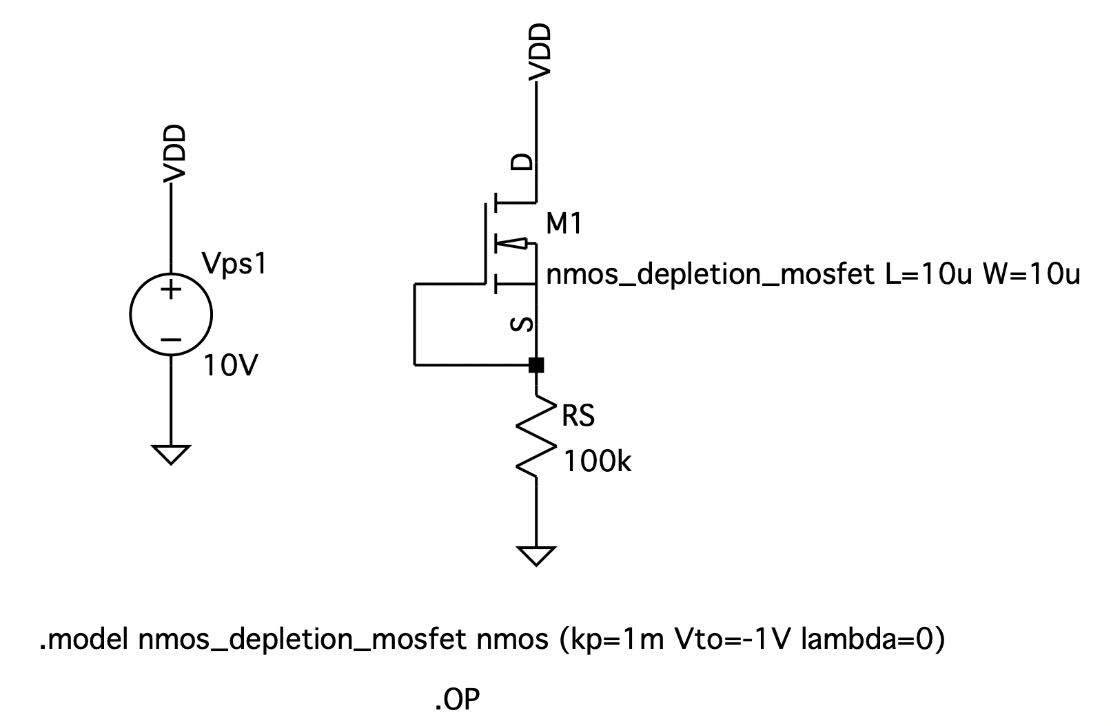
5.2.3 A Depletion-Mode N-Channel MOSFET Circuit
As the final example of this section, we shall look at a circuit containing a depletion-mode NMOS transistor. Consider the circuit shown in Fig. 5.13 where M1 is assumed to have the following parameters: Vt=-1 V, 𝜇n COX=1 mA/V2}, and 𝜆=0. The LTSpice generated circuit netlist corresponding to this circuit is listed in Fig. 5.15 and the results of an operating point analysis (.OP) are presented, in part, below:
|
Semiconductor Device Operating Points:
--- MOSFET Transistors --- Name: m1 Model: nmos_depletion_mosfet Id: 9.90e-05 Vgs: 0.00e+00 Vds: 1.04e-01 Vbs: 0.00e+00 Vth: -1.00e+00 Vdsat: 1.00e+00
Operating Bias Point Solution:
V(d) 10 voltage V(s) 9.89559 voltage Id(M1) 9.89551e-05 device_current Ig(M1) 0 device_current Ib(M1) -1.14229e-13 device_current Is(M1) -9.89551e-05 device_current I(Rs) 9.89559e-05 device_current I(Vps1) -9.89559e-05 device_current
|
Notice that in this case vDS < VDS,SAT, implying that the transistor is operating in the triode region.
In the following, we repeat the above analysis with the same MOSFET model used above with the addition that it has a channel-length modulation coefficient lambda equal to 0.04 V-1. On doing so, we find in the Spice Error Log output file the following DC operating information:
|
Semiconductor Device Operating Points:
--- MOSFET Transistors --- Name: m1 Model: nmos_depletion_mosfet Id: 9.90e-05 Vgs: 0.00e+00 Vds: 1.04e-01 Vbs: 0.00e+00 Vth: -1.00e+00 Vdsat: 1.00e+00
Operating Bias Point Solution:
V(d) 10 voltage V(s) 9.89605 voltage Id(M1) 9.89603e-05 device_current Ig(M1) 0 device_current Ib(M1) -1.13774e-13 device_current Is(M1) -9.89603e-05 device_current I(Rs) 9.89605e-05 device_current I(Vps1) -9.89605e-05 device_current
|
Thus, we see that only the voltage at the source node has changed to 9.8960 V from the previous value of 9.8956 V. All other values listed appear to be the same as before; given the 3 or 4 digits of accuracy. Thus, the inclusion of the term lambda term does not seem to affect the behavior of the circuit significantly when the device is operated in the triode region.
5.3 Describing JFETs To Spice
Like MOSFETs, JFETs are described to Spice using an element statement and a model statement. The following outlines the syntax of these two statements, including the details of the built-in JFET model.
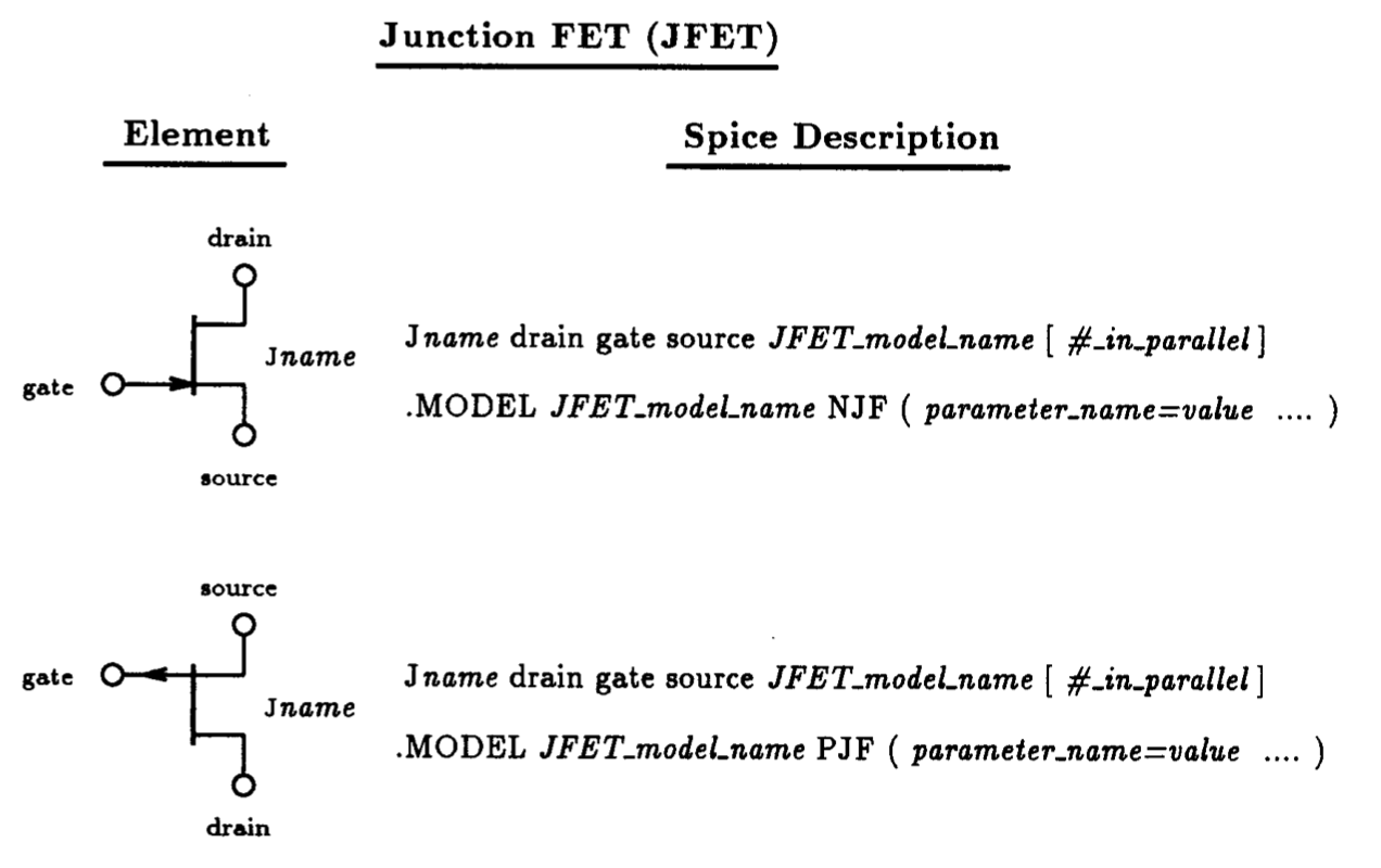
Fig. 5.15: Spice element description for the n-channel and p-channel JFETs. Also listed is the general form of the JFET model statement. A partial listing of the parameters applicable to either an n-channel or p-channel JFET is given in Table 5.2.
5.3.1 JFET Element Description
JFETs are describe to Spice using an element statement beginning with a unique name prefixed with the letter J. This is then followed by a list of the nodes that the drain, gate, and source of the JFET are connected to. The next field specifies the name of the model that characterizes its terminal behavior, and the final field of this statement is optional, and its purpose is to allow one to scale the size of the device by specifying the number of JFETs connected in parallel. A summary of the element statement syntax for both the n-channel and p-channel JFETs is provided in Fig. 5.15. Included in this list is the syntax for the JFET model statement (.MODEL). This statement defines the terminal characteristics of the JFET by specifying the values of parameters in the JFET model. Parameters not specified in the model statement are assigned default values by Spice. Details of this model will be discussed briefly next.
|
Fig. 5.16: The Spice large-signal n-channel JFET model under static conditions.
|
Table. 5.2: A partial listing of the Spice parameters for the JFET model.
|


5.3.2 JFET Model Description
As is evident from Fig. 5.15, the model statement for either the n-channel or p-channel JFET transistor begins with the keyword .MODEL and is followed by the name of the model used by a JFET element statement, the nature of the JFET (i.e., NJF or PJF), and a list of the JFET parameter values (enclosed between brackets). Specifically, the mathematical model of the JFET in Spice is very similar to that seen earlier for the Level 1 MOSFET model.
The general form of the DC Spice model for an n-channel JFET is illustrated schematically in Fig. 5.16. The bulk resistance of the drain and source regions of the JFET are lumped into two linear resistances rD and rS, respectively. The DC characteristic of the intrinsic JFET is determined by the nonlinear dependent current source iD, and the two diodes represent the two substrate junctions that define the channel region. A similar model applies for the p-channel device; the direction of the diodes, the current source and the polarities of the terminal voltages are all reversed. The expression for drain current iD, assuming that the drain is at a higher potential than the source, is described by the following:
where the device parameters b and Vt are written in terms of IDSS and VP as
(5.5)

and
(5.6)
From the above, we see that the JFET has 3 parameters that define its operation: IDSS, VP and lambda. The parameter IDSS is the drain current when VGS=0 V, and VP corresponds to the pinch-off voltage of the channel. The parameter lambda is the channel-length modulation parameter and represents the influence that the drain-source voltage has on the drain current iD when the device is in pinch-off. The sign of this parameter is always positive, regardless of the nature of the device type. A note on notation: The transconductance coefficient beta is denoted by the parameter K in some textbooks.
A partial listing of the parameters associated with the Spice JFET model under static conditions is given in Table 5.2. Also listed are the default values which the parameter assume if no value is specified on the .MODEL statement. To specify a parameter value one simply writes, for example: beta=1m, Vto=-1V, 𝜆=0.01, etc.
|
(a)
(b)
Fig. 5.17: An n-channel JFET circuit example. (a) circuit schematic, and (b) LTSpice captured circuit.
|
A Simple N-Channel JFET Circuit * * Circuit Description * * dc supplies Vps1 VDD 0 10V * JFET circuit J1 D 0 S n_jfet RD VDD D 1k RS S 0 0.5k * n-channel jfet model statement .model n_jfet NJF (beta=1m Vto=-4V lambda=0) * unused model related statements .model NMOS NMOS .model PMOS PMOS .lib /Users/roberts/Library/Application Support/LTspice/lib/cmp/standard.jft * * Analysis Requests * * calculate DC bias point .OP .backanno .end
Fig. 5.18: The Spice input file for calculating the DC operating point of the JFET circuit shown in Fig. 5.17.
|


5.3.3 An N-Channel JFET Example
To demonstrate how a circuit containing a JFET is described to LTSpice, consider the circuit shown in Fig. 5.17(a). Here the JFET is n-channel with parameters: VP=-4 V, IDSS=16 mA and 𝜆=0. The model statement for this particular n-channel JFET would be described as follows:
.model n_jfet NJF (beta=1m Vto=-4V lambda=0)
In this particular case, one had to convert the device parameters into terms that LTSpice is familiar with. This required that one compute beta from IDSS and VP according to beta = IDSS/VP2. Vt is simply equal to VP.
In keeping with the discussion thus far, we shall compute the DC operating point of the circuit shown in Fig. 5.17. The LTSpice schematic captured circuit, including the appropriate analysis request (i.e., .OP command), can be seen in Fig. 5.17(b). On execution, the following results are found in the Spice Error Log file:
|
Semiconductor Device Operating Points:
--- JFET Transistors --- Name: j1 Model: n_jfet Id: 4.00e-03 Vgs: -2.00e+00 Vds: 4.00e+00
Operating Bias Point Solution:
V(vdd) 10 voltage V(d) 6 voltage V(s) 2 voltage Id(J1) 0.004 device_current Ig(J1) -8.02e-12 device_current Is(J1) -0.004 device_current I(Rs) 0.004 device_current I(Rd) 0.004 device_current I(Vps1) -0.004 device_current
|
Here we see that the JFET is biased with a drain current of 4 mA and that the drain is at a voltage of 6 V.
|
Fig. 5.19: A p-channel JFET circuit as captured by LTSpice.
|
A Simple P-Channel JFET Circuit
** Circuit Description ** * dc supplies Vps1 VDD 0 5V Vps2 0 VSS 5V IB VDD S 1mA * JFET circuit J1 D 0 S p_jfet RD D VSS 2k * p-channel jfet model statement .model p_jfet PJF (beta=1m Vto=-2V lambda=0) * unused model related statements .model NMOS NMOS .model PMOS PMOS .lib /Users/roberts/Library/Application Support/LTspice/lib/cmp/standard.jft * * Analysis Requests * * calculate DC bias point .OP .backanno .end
Fig. 5.20: The Spice input file for calculating the DC operating point of the p-channel JFET circuit shown in Fig. 5.19.
|

5.3.4 A P-Channel JFET Example
This next example is along the same lines as the previous JFET example except that the JFET is p-channel. The p-channel JFET circuit that we will analyze for its DC bias conditions using a .OP directive and captured by LTspice is on display in Fig. 5.19. Here the p-channel device has parameters: VP=+2 V, IDSS=4 mA and 𝜆=0. The importance of this example is to highlight the fact that the threshold voltage (Vt) of the p-channel JFET is specified on the model statement as a negative value, even though VP is positive. One must be careful of this for it is opposite to what is used in many undergraduate textbooks. The rationale for this is that the originators of Spice adopted the convention that a depletion-mode device, which the JFET is, would have Vt < 0 whether it be n-channel or p-channel. The model statement for this particular p-channel JFET would be described as follows:
.model p_jfet PJF (beta=1m Vto=-2V lambda=0).
The LTSpice generated circuit netlist is shown in Fig. 5.20. On execution of LTSpice, the following results are found in the Spice Error Log file:
|
Semiconductor Device Operating Points:
--- JFET Transistors --- Name: j1 Model: p_jfet Id: -1.00e-03 Vgs: 1.00e+00 Vds: -2.00e+00 Gm: 2.00e-03 Gds: 0.00e+00 Cgs: 0.00e+00 Cgd: 0.00e+00
Operating Bias Point Solution: V(vdd) 5 voltage V(d) -3 voltage V(vss) -5 voltage V(s) -1 voltage I(Ib) 0.001 device_current Id(J1) -0.001 device_current Ig(J1) 4.02e-12 device_current Is(J1) 0.001 device_current I(Rd) 0.001 device_current I(Vps2) -0.001 device_current I(Vps1) -0.001 device_current |
As is evident, the transistor is biased at 1 mA, and the source and drain are at -1 V and -3 V, respectively.
To see how much the DC bias calculation changes with the inclusion of the transistor channel-length modulation effect, we repeat the above analysis with lambda=0.04 V-1. Modifying the LTSpice schematic shown in Fig. 5.19 to reflect this change, we then re-execute. The following results are then obtained:
|
Semiconductor Device Operating Points:
--- JFET Transistors --- Name: j1 Model: p_jfet Id: -1.00e-03 Vgs: 1.04e+00 Vds: -1.96e+00 Gm: 2.08e-03 Gds: 3.71e-05 Cgs: 0.00e+00 Cgd: 0.00e+00
Operating Bias Point Solution: V(vdd) 5 voltage V(d) -3 voltage V(vss) -5 voltage V(s) -1.03709 voltage I(Ib) 0.001 device_current Id(J1) -0.001 device_current Ig(J1) 4.05709e-12 device_current Is(J1) 0.001 device_current I(Rd) 0.001 device_current I(Vps2) -0.001 device_current I(Vps1) -0.001 device_current
|
Since the JFET is biased externally with a current source the effect of the channel-length modulation will manifest itself in the voltages that appear across the terminals of the device. For instance, the gate-source voltage increases from 1 V to 1.04 V. Likewise, the drain-source voltage experiences the same voltage change. In both cases, the resulting voltage change is small, and this provides further justification that it is reasonable to neglect the presence of channel-length modulation when performing DC bias calculations by hand.
5.4 FET Amplifier Circuits
Field-effect transistors are commonly employed in the design of linear amplifiers. Small-signal linear analysis is commonly employed as a means of estimating various attributes of amplifier behavior when subjected to small input signals. Examples of amplifier attributes would include input and output resistances, and current and voltage signal gain. LTSpice has a small-signal linear model of the MOSFET and another for the JFET. We shall describe these in this section. Subsequently, we shall illustrate the effectiveness of small-signal analysis as it applies to a common-source n-channel enhancement-mode MOSFET amplifier. This is accomplished by comparing the results calculated by hand with those generated by Spice. But before these undertakings, we shall illustrate the importance of biasing a FET around an operating point that is well within the saturation region of the device.
|
(a) |
(b) |
|
Fig. 5.21: Dynamic amplifier behavior: (a) A fixed-bias n-channel MOSFET amplifier configuration, and (b) Circuit captured by LTSpice.
|
|

|
Fig. 5.22: LTSpice curve-tracer circuit arrangement to analyze the transfer characteristic of an NMOS transistor. Also, the circuit arrangement used to compute the load line for the amplifier under different loads is provided. |
Fig. 5.23: The iD-vDS characteristics of an n-channel MOSFET having model parameters Vt=+2 V, 1/2unCOX(W/L)=1 mA/V2 and lambda=0.01 V-1. Load lines for the MOSFET amplifier shown in Fig. 5.22 for drain resistances of 1.33 kW and 1.78 kW. Q1 and Q2 indicate the DC operating point of each amplifier with a gate-source bias voltage of 5 V.
|


|
(a) |
(b) |
|
Fig. 5.24: The input and output large-signal transient behavior of the MOSFET amplifier shown in Fig. 5.22 for a drain/load resistance of: (a) 1.33 kW (b) 1.78 kW.
|
|


5.4.1 Effect of Bias Point on Amplifier Conditions
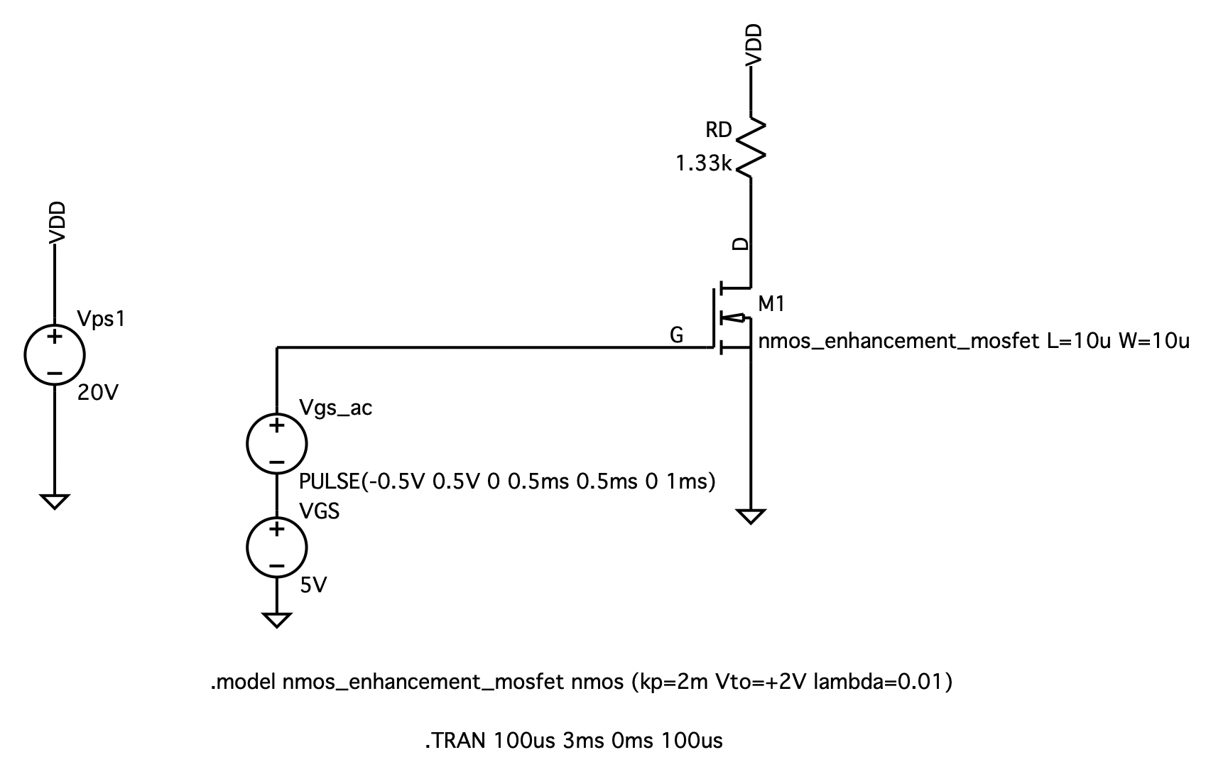
In this section we consider the effect that a misplaced DC operating point has on the large-signal operation of the MOSFET amplifier shown in Fig. 5.21(a). For the enhancement-type n-channel MOSFET amplifier shown in Fig. 5.21(a) with a +5 V fixed gate-biasing scheme operating, 20 V power supply, the DC operating point of the MOSFET has been set at approximately ID=9 mA and vDS=8 V. This is a result of the MOSFET having an assumed threshold voltage Vt of +2 V, a conductance parameter K= 1/2𝜇nCOX(W/L)=1 mA/V2 and a channel-length modulation factor lambda=0.01 V-1. The aspect ratio of the transistor is assumed to be L=W=10 𝜇m. The circuit was entered into LTSpice using the schematic capture method and is shown in Fig. 5.21(b). Here a 1 V peak-to-peak triangular waveform of 1 kHz frequency is placed in series with the 5 V DC biasing voltage. This source will be used to evaluate the dynamic behavior of the amplifier.
Before completing the analysis of the amplifier of Fig. 5.21, let us consider the transfer characteristic of the NMOS device that is to be used in the amplifier of Fig. 5.21. This is found by sweeping the gate and drain voltages independently of one another using a nested .DC sweep command, as illustrated in Fig. 5.22. Also, included are two resistors (1.33 kΩ and 1.78 kΩ) connected between the drain terminal and a 20 V power supply. By monitoring the current through each resistor, the load line for each load can be superimposed on the DC transfer characteristic of the transistor, as shown in Fig. 5.23. For a gate-source voltage of 5 V, the load line and NMOS curves intersect at two points, Q1 and Q2. Q1 indicates the operating point for the 1.33 kΩ load, and Q2 indicates the operating pointy go the 1.78 kΩ load. This is shown in Fig. 5.23. Here one can see that the operating point Q1 is located slightly to the left of the midway point between the triode and cut-off regions. For a load of 1.78 kΩ, the DC operating point, Q2, moves closer to the edge of the triode region.
To illustrate the effect that the location of the DC operating point has on the large-signal behavior of the amplifier, consider comparing the input-output behavior of the amplifier operating at Q1 and Q2 subject to a 1-V, 1 kHz triangular input. A transient analysis command is necessary to compute the behavior of this amplifier over a 3-ms time interval. This too can be seen written on the schematic of Fig. 5.21(b). To begin, the load resistor is set to 1.33 kΩ and the transient analysis is performed. The load resistor is then change to 1.78 kΩ and the transient analysis is run again. The corresponding results are shown in Fig. 5.24(b). For a drain resistance of 1.33 kΩ, the output waveform is a scaled version of the input triangular signal; about 6.8 times the input signal, albeit, with a negative gain. This is in contrast with the case when the drain resistance is increased to 1.78 kW where we see in Fig. 5.24(b) that the output signal has become quite distorted in the lower portion of its waveform. Thus, this example helps to illustrate the importance of placing the DC operating point of an amplifier well within the saturation region of the MOSFET in order to maximize the output voltage swing of the amplifier while maintaining linear operation.
|
(a) |
(b) |
|
Fig. 5.25: The static Spice small-signal model of: (a) MOSFET, (b) JFET.
|
|


5.4.1 Small-Signal Model of the FET
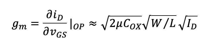
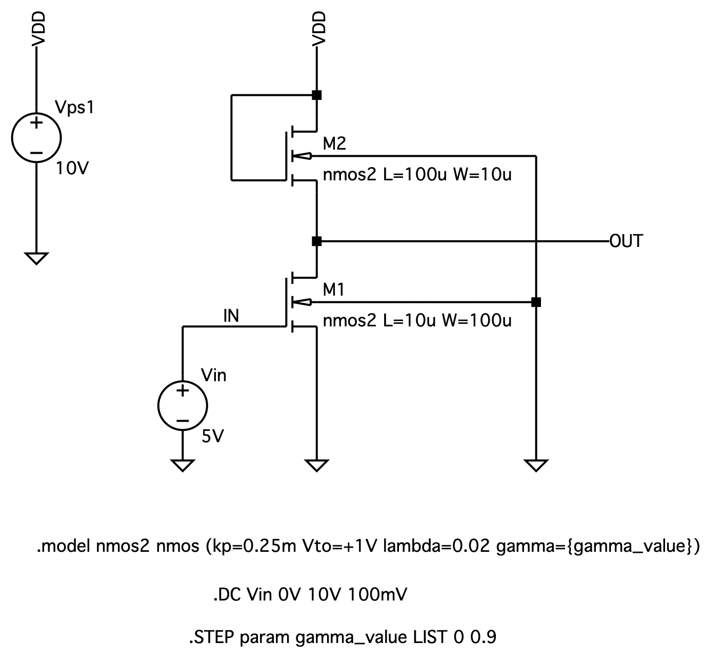
The linearized small-signal model for the MOSFET is shown in Fig. 5.25(a). It consists of two voltage-controlled current sources with transconductance gm and gmb. The MOSFET transconductance, gm, is related to the DC bias current ID and the device parameters (ignoring the channel-length modulation effect) as follows:
(5.7)
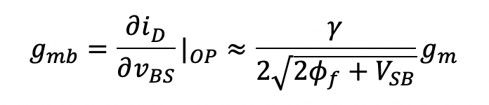
Here |OP indicates that the derivative is obtained at the DC operating point of the device. The next term, gmb, is known as the body transconductance and is related to several MOSFET bias conditions and device parameters according to:
(5.8)
Accounting for the presence of channel-length modulation, the output conductance gds, which is also equal to 1/ro, is given approximately by the expression
(5.9)

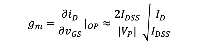
Finally, the resistances rD and rS represent the ohmic resistance of drain and source regions, respectively. The small-signal linear model of a JFET is shown in Fig. 5.25(b). It consists of a single voltage-controlled current source having a transconductance gm that is related to the DC bias current ID and device parameters (ignoring the channel-length modulation effect) according to the following:
(5.10)
Accounting for the presence of channel-length modulation, the output conductance gds, which is also equal to 1/ro, is given approximately by the expression
(5.11)

Lastly, the resistances rD and rS represent the ohmic resistance of the drain and source regions, respectively.
Many of the analysis that is performed on a transistor circuit by LTSpice utilizes its linear small-signal equivalent circuit. The parameters of the small-signal model of each transistor in a given circuit, as computed by LTSpice, are available to the user through the operating point (.OP) command. To see this, consider a single NMOS transistor with its drain biased at +5 V, its gate biased at +3 V, and its source connected to ground. Furthermore, we shall assume that the substrate is biased at -5 V. The transistor is assumed to have the following parameters: Vt0=+1 V, 𝜇nCOX= 20 𝜇A/V2, L=10 𝜇m, and W=400 𝜇m. Furthermore, lambda=0.05 V-1 and g=0.9 V1/2. The LTSpice circuit netlist for this circuit is provided below:
|
Small-Signal Model Of An N-Channel MOSFET * * Circuit Description * * mosfet terminal bias Vd 1 0 DC +5V Vg 2 0 DC +3V Vb 3 0 DC -5V * mosfet under test M1 1 2 0 3 nmos_enhancement_mosfet L=10u W=400u * mosfet model statement (by default, level 1) .model nmos_enhancement_mosfet nmos (kp=20u Vto=1V lambda=0.05 gamma=0.9) * * Analysis Requests * .OP .end
|
On execution of LTSpice, one finds in the Spice Error Log file the following complete list of parameters pertaining to the small-signal MOSFET model computed by LTSpice:
|
Semiconductor Device Operating Points:
--- MOSFET Transistors --- Name: m1 Model: nmos_enhancement_mosfet Id: 1.61e-04 Vgs: 3.00e+00 Vds: 5.00e+00 Vbs: -5.00e+00 Vth: 2.43e+00 Vdsat: 5.67e-01 Gm: 5.67e-04 Gds: 6.44e-06 Gmb: 1.08e-04 Cbd: 0.00e+00 Cbs: 0.00e+00 Cgsov: 0.00e+00 Cgdov: 0.00e+00 Cgbov: 0.00e+00 Cgs: 0.00e+00 Cgd: 0.00e+00 Cgb: 0.00e+00
|
Included in the above list of operating point information are: (a) DC bias conditions which include drain current and various terminal voltages; (b) device transconductances gm and gmb; (c) output conductance gds; and (d) device capacitances accounting for MOSFET dynamic effects. All the parameters in this list, except for the capacitances (these are all zero for the time being), have been discussed previously and therefore their meaning should be self-evident. A discussion of MOSFET capacitances will be deferred until Chapter 7.
Similar results extend to the JFET. We leave this to the reader to confirm.
|
(a)
|
(b)
|
|
Fig. 5.26: A common-source amplifier circuit: (a) schematic, and (b) circuit schematic captured by LTSpice for .OP analysis.
|
|


|
|
|
|

5.4.2 A Basic FET Amplifier Circuit
Fig. 5.26(a) displays an enhancement-mode NMOS amplifier in which the input signal vI is coupled to the gate of the MOSFET through a large capacitor, and the output signal at the drain is coupled to the load resistance RL via another large capacitor. The MOSFET is assumed to have device parameters: Vt=+1.5 V, 𝜇COX=0.25 mA/V2 and 𝜆=0.02 V-1. The dimensions of the MOSFET is L=W=10 𝜇m. This same example was analyzed by hand analysis where it was found that this amplifier would have a voltage gain of -3.3 V/V and an input resistance of 2.33 MW. These results were obtained by performing a small-signal analysis of the amplifier circuit through a two-step procedure. The first step was to obtain the DC bias conditions of the circuit, specifically the drain current, from which the small-signal model for the transistor is obtained. The second step was to analyze the linear small-signal equivalent circuit of the amplifier to obtain the voltage gain and the input resistance. In each step of the analysis some simplifying assumptions are made. For instance, during the DC bias calculation, the transistor channel-length modulation effect was ignored. In the second step, a simplifying assumption was made with regards to the current flowing through the feedback resistor RG. We have seen in previous examples of this chapter that ignoring the channel-length modulation effect results in small variations in the drain current of a MOSFET, and thus, by extension, variations in the small-signal model parameters would also be small. In the following, with the aid of LTSpice, we would like to investigate the accuracy of these two steps as they apply to the common-source amplifier in Fig. 5.26(a) and demonstrate that these simplifying assumptions are reasonable.
According to our hand analysis (which ignores the channel-length modulation effect) the drain current of the MOSFET is 1.06 mA. Thus, from Eqns. (5.7) and (5.11) the MOSFET transconductance gm equals 0.725 mA/V and the output resistance ro is equal to 47 kW. To compare these results to those calculated by LTSpice, the circuit was captured by LTSpice as shown in Fig. 5.26(b). The infinite-valued coupling capacitors are represented by 1 farads. This will ensure that the capacitors behave as short circuits at the signal frequencies of interest. Remember to NOT include an F for farard, as LTSpice will parse it as a 10-15 multiplier. On executing a dc analysis using a .OP directive, results in the small-signal data as follows:
|
Semiconductor Device Operating Points:
--- MOSFET Transistors --- Name: m1 Model: nmos1 Id: 1.07e-03 Vgs: 4.31e+00 Vds: 4.31e+00 Vbs: 0.00e+00 Vth: 1.50e+00 Vdsat: 2.81e+00 Gm: 7.62e-04 Gds: 1.97e-05 Gmb: 0.00e+00
|
Here we see that the MOSFET is biased at a drain current of 1.07 mA, has a transconductance gm equal to 0.762 mA/V and an output conductance of 19.7 𝜇S, or an output resistance ro of 50.8 kW. Comparing the hand calculated values with those generated by LTSpice, we see that the hand calculated results are quite close, with at most, a 7.5% error. In Table 5.3 we list these two sets of results and also list the relative error between them.
|
Table. 5.3: Comparing the transistor drain current ID and its corresponding small-signal model parameters gm and ro as computed by straightforward hand analysis and LTSpice. |

Once the small-signal equivalent circuit of the amplifier is obtained, one proceeds to analyze the circuit using standard circuit analysis techniques to obtain pertinent amplifier parameters, such as voltage gain and input resistance. To gain insight into circuit behavior, closed-form expressions are usually derived from the equivalent circuit. In many cases, the expressions that result are complicated, large, and not very insightful. As a result, one makes simplifying assumptions based on practical considerations that lead to expressions that are simpler, but more insightful. For example, the linear small-signal equivalent circuit of the common-source amplifier shown in Fig. 5.26(a) was analyzed and the following expressions for its voltage gain and input resistance were obtained after making several practical assumptions:
(5.12)
![]()
and
(5.13)

It is the simplicity of these two formulas that makes them useful in circuit design. The question then becomes: How accurate are they?
To verify their accuracy, we simply substitute the appropriate circuit parameters, together with the small-signal parameters of the MOSFET generated by LTSpice above and evaluate. This is then compared with the results computed directly by LTSpice. For the first part, we find AV=-3.468 V/V and Rin=2.238 kW. With regard to the analysis we ask LTSpice to perform, one might be tempted to request a transfer function (.TF) analysis and directly obtain both the small-signal voltage gain and the amplifier input resistance. Unfortunately, the amplifier is AC coupled and intended to amplify signals containing frequencies other than DC. Since the .TF analysis calculates the small-signal input - output behavior of a circuit only at DC, in the situation at hand the results produced would not prove very useful. Instead, we shall apply a one-volt AC voltage signal to the input of the amplifier (source Vin is modified) and compute the voltage appearing at the amplifier output using the .AC analysis command of LTSpice at a single midband frequency of, say, between 1 Hz – 100 kHz using the following directive:
.AC DEC 10 1Hz 100kHz
A one-volt input level is usually chosen here because, in this way, the output voltage would be directly equal to the input-output transfer function. The input signal level of one-volt is not considered to be above the small-signal limit of the amplifier because the .AC analysis performed by LTSpice is performed directly with the small-signal equivalent circuit of the amplifier. Thus, any input level would work.
In a similar vein, from the same analysis, we can also use the waveform viewer to compute the input resistance of amplifier by plotting the ratio of the input voltage to input current.
The relevant AC analysis results computed by LTSpice are displayed in Fig. 5.27. The magnitude of the small-signal voltage gain of the amplifier (AV) is therefore 3.466 V/V and the input resistance Rin is 2.238 MW.
|
Table. 5.4: Comparing the voltage gain and the input resistance of the amplifier shown in Fig. 5.26 as calculated by three different methods: (a) closed-form expression using hand estimates of the small-signal model parameters; (b) closed-form expression using Spice calculated small-signal model parameters; (c) direct calculation using Spice.
|

Comparing these two sets of results, one set derived using hand analysis together with LTSpice generated small-signal model parameters (-3.468 V/V, 2.238 MW), and the other derived directly using LTSpice (-3.476 V/V, 2.238 MW), we see that these results are either identical to one another or quite close with a relative error of only 0.23%. We can therefore conclude that the simplifying assumptions used to derive the formula for small-signal voltage gain and input resistance are very reasonable and introduce very little error. When the small-signal parameters computed by hand are used instead of the LTSpice generated model parameters, the accuracy of the results decrease but remain within practical limits (i.e., AV=-3.3 V/V and Rin=2.33 MW). The relative error of the two calculations are in the vicinity of 5%. This error is largely due to the error incurred through the DC hand analysis which ignored the transistor channel-length modulation effect. A summary of the above discussion is provided in Table 5.4 for easy reference.
|
(a) |
(b) |
|
Fig. 5.28: Two different MOSFET biasing arrangements: (a) fixed biasing, and (b) biasing with source resistance feedback. |
|


|
|
|
Fig. 5.29: LTSpice circuit capture for comparing the sensitivity of its biasing circuit on the transistor current level using a Monte Carlo analysis. The circuit on the left involves a transistor biasing arrangement with fixed biasing (no RS), whereas the circuit on the right implements the biasing using source resistance feedback (with RS). All resistors are assumed to vary about a nominal value with a uniformly distribution having a ±5% variation. Both circuits operate at a drain voltage very near 9 V and at the same drain current. |

|
|
|
Fig. 5.30: The drain currents of the amplifier with and without RS when all biasing resistors are varied by ±5% their nominal values. Clearly, the circuit with RS has lower bias current sensitivity to resistor variations than the one with RS included.
|

|
|
|
Fig. 5.31: Variations in the drain currents of the amplifier with and without RS subject to variation in the power Supply level, VDD. Clearly, the circuit with RS has lower power supply sensitivity to resistor variations than the one with RS included.
|

|
|
Fig. 5.32: Variations in the drain currents of the amplifier with and without RS subject to variation in NMOS model parameter Vto. Clearly, the circuit with RS has lower power supply sensitivity to resistor variations than the one with RS included. |

5.5 Investigating Bias Sensitivity Using A Monte Carlo Analysis
To obtain a stable DC operating point in discrete transistor circuits, a biasing scheme utilizing some form of negative feedback is usually employed. This ensures that the DC bias currents through the transistors in the circuit remain relatively constant under the influence of normal manufacturing or environmental variations.
To illustrate the effectiveness of incorporating negative feedback in the biasing network of a transistor amplifier, let us perform a Monte Carlo analysis on the two circuits shown in Fig. 5.28. The full details of the Monte Carlo analysis were first outline in Section 4.7. Each MOSFET will be assumed to have the following parameters: Vt=+2 V, 𝜇nCOX=2 mA/V2 and 𝜆= 0. For a fair comparison, each amplifier is biased at approximately the same current level of 3 mA. The n-channel enhancement MOSFET amplifier of Fig. 5.28(a) is simply biased by a voltage appearing at its gate terminal. Although, the MOSFET in the amplifier of Fig. 5.28(b) is also biased with a voltage at its gate through a voltage divider circuit, a resistor is included in the source lead of the MOSFET which provides a feedback action that acts to stabilize the drain current of the MOSFET when subjected to change. What this means is, if one of the biasing elements undergoes a small change, then the resulting drain current of the MOSFET will experience less change than when no feedback action is present. To see this, the two circuits are captured into one LTSpice schematic and all resistors are assigned a value that is randomly selected from a uniform distribution whose average value is set to the nominal component value (i.e., a value that provides a 3 mA drain current level) bounded between ±5% of this nominal value. This is achieved by setting the value of each component using a mc function call between brackets. For example, if the nominal resistor value is 1 kΩ, then the random variable will be selected from a uniform distribution bounded between 950 to 1050. The function call would then be written as {mc(1k,0.05)}. To collect statistically significant data, the DC analysis driven by the .OP command will be repeated 101 times. This is achieved using the following .STEP command:
.STEP param run 1 101 1
The Monte Carlo setup used in LTSpice for this circuit comparison is shown in Fig. 5.29. On execution and observing the drain currents of the two amplifier circuits across the different runs results in the plot shown in Fig. 5.30. As is evident from this plot, the circuit without a source resistor experiences about 10 times more variation than the circuit that uses a source resistance (i.e., 1.8 mA versus 0.2 mA peak-to-peak variation). Clearly, the application of the localized feedback provided by the source resistor provides much better bias sensitivity.
This same type of analysis can be repeated with regards to a variation in the supply voltage VDD. Resetting the resistor values in Fig. 5.28 to their nominal values, and inserting an mc function call in the power supply Vps1 value to {mc{15,0.01)}, the drain current for the two circuits can be seen in Fig. 5.31. As is evident, the circuit without RS experiences a 241 uV peak-to-peak variation when the power supply varies by ±1% of 15 V, which is equivalent to 150 mV peak-to-peak. Thus, the circuit has a power supply gain of 241 𝜇V / 150 mV, or 1.6 mV/V. Conversely, the circuit with RS experiences an 80 𝜇V peak-to-peak change. Thus, this circuit has a power supply gain of 80 𝜇V / 150 mV, or 0.533 mV/V. This is a three times improvement. Yet again, the simulation results confirm that the biasing arrangement that use localized feedback is better than one that uses a fixed biasing or no localized feedback
A Monte Carlo analysis can be applied to model variations in transistor model parameters. For instance, if the power supply and resistors are all reset to their nominal values, and the model statement is revised such that the threshold voltage is assigned a random variable using the mc function call, i.e.,
.model nmos1 nmos (kp=2m Vto={mc(2,0.05)} lambda=0)
then the effects of variation in the MOSFET threshold voltage can be investigated. On doing so, the results are shown in Fig. 5.32. The results again suggest localized feedback biasing is best. Other device parameters could also be investigated using a Monte Carlo analysis. This is left for the reader to pursue.
5.6 Integrated-Circuit MOS Amplifiers
In this section we shall investigate the behavior of several different types of fully integratable amplifiers that are constructed with MOSFETs only.
|
Fig. 5.33: An enhancement-load amplifier.
|
Fig. 5.34: The LTSpice schematic for calculating the DC transfer characteristic of the enhancement-load amplifier shown in Fig. 5.33. Through the application of a .STEP directive, the body effect can be incorporated with different values.
|

|
Fig. 5.35: The DC transfer characteristic of the enhancement-load amplifier shown in Fig. 5.32 with and without the MOSFET body-effect present.
|
Fig. 5.36: The input-output voltage gain of the enhancement-load amplifier shown in Fig. 5.32 with and without the MOSFET body-effect present. The x-axis represents the body-effect gamma value.
|


5.5.1 Enhancement-Load Amplifier Including the Body Effect
Fig. 5.33 shows an enhancement-load NMOS amplifier with the substrate connections clearly shown. This arrangement would be typical of an amplifier implemented in an NMOS fabrication process. One important drawback to this amplifier is that its voltage gain is reduced because of the presence of the MOSFET body-effect in transistor M2. To see this, let us consider that the two MOSFETs in the circuit of Fig. 5.33 have the following device parameters: a process transconductance coefficient (𝜇nCOX) of 0.25 mA/V2, a zero-bias threshold voltage of 1 V, a channel-length modulation factor lambda of 0.02 V-1, and a body-effect coefficient gamma of 0.9 V1/2. Transistor M1 will have a length - width dimension of 10 𝜇m by 100 𝜇m whereas the dimensions of transistor M2 will be reciprocated at 100 𝜇m by 10 𝜇m. A DC sweep of the input voltage level between ground and VDD is requested. For comparison, we shall repeat the same analysis just described on an identical circuit, with identical device parameters except that the body-effect coefficient will be set to zero. This is achieved using the following three Spice directives that modifies the gamma value set in the NMOS model statement, i.e.,
.model nmos2 nmos (kp=0.25m Vto=+1V lambda=0.02 gamma={gamma_value})
.DC Vin 0V 10V 100mV
.STEP param gamma_value LIST 0 0.9
The results of the analysis are shown in Fig. 5.35. Here the DC transfer characteristics of the enhancement-load amplifier with and without the transistor body-effect present are shown. As is clearly evident, transistor body-effect alters the transfer characteristics of the enhancement-load amplifier significantly. With the input level below one-volt, corresponding to the threshold of M1, the output voltage is held constant at either 9 V or 7.2 V, depending on which characteristic curve one is looking at. In the case of the transfer characteristic curve for the enhancement-load circuit with the body-effect present, with input levels increasing above the one-volt level, the output voltage decreases linearly at a rate of about -7.9 volt-per-volt from its initial 7.2 V level until the input exceeds approximately 1.8 V. At an input of 1.8 V the output is 0.75 V. Above this input voltage level, transistor M1 leaves the saturation-region and enters the triode region, resulting in the amplifier characteristics becoming nonlinear.
In the case of the amplifier with the body-effect eliminated, with inputs above 1 V, the output level (beginning at 9 V) decreases linearly at a rate of -9.2 volt-per-volt. Like the previous case, when the input voltage level exceeds 1.8 V (and the output at 0.75 V), transistor M1 enters the triode region and the amplifier characteristic curve becomes nonlinear. Comparing these details to that of the enhancement-load amplifier with the body-effect included suggest that the presence of transistor body-effect has decreased the effective gain of this enhancement-load amplifier.
To further demonstrate this, let us compute the voltage gain of this amplifier, with and without the body-effect present, using the transfer function (.TF) analysis command of Spice with the amplifier biased in its linear region. For illustrative purposes, we shall bias the input to the amplifier at 1.5 V since this input level maintains both amplifiers in their linear region. Modifying the LTSpice schematic used previously, by changing the source statement to have a DC value of 1.5 V and include the following .TF command
.TF V(OUT) Vi.
Further, we shall sweep the body-effect coefficient from 0 to 1.0 V1/2 in increments of 0.1 V1/2 using the following .STEP directive:
.STEP param gamma_value 0 1.0 0.1
The results of this analysis are shown in Fig. 5.36. As is evident, as the body-effect coefficient gamma increases the magnitude of the gain of an enhancement-load amplifier decreases.
Before we leave this section, it would be instructive to confirm that the small-signal formula for the voltage gain of this amplifier including transistor body-effect, given below, is accurate:
(5.14)
Through an operating point (.OP) analysis command, we find the following values for the small-signal model parameters of each transistor with Vin = 1.5 V and gamma = 0.9 V1/2:
|
Semiconductor Device Operating Points:
--- MOSFET Transistors --- Name: m2 m1 Model: nmos2 nmos2 Id: 3.32e-04 3.32e-04 Vgs: 6.87e+00 1.50e+00 Vds: 6.87e+00 3.13e+00 Vbs: -3.13e+00 0.00e+00 Vth: 2.04e+00 1.00e+00 Vdsat: 4.83e+00 5.00e-01 Gm: 1.37e-04 1.33e-03 Gds: 5.84e-06 6.25e-06 Gmb: 3.20e-05 7.72e-04 |
Substituting the appropriate values into Eqn. (5.14), we find AV=-7.344 V/V. This is very close to the value predicted directly by LTSpice above (i.e., AV=-7.316 V/V). If the output conductance’s are neglected in this calculation, then we would find AV=-7.869 V/V. This result, for most practical applications, would be more than adequate.
|
(a)
(b)
Fig. 5.37: A CMOS amplifier with current source biasing. (a) schematic circuit, (b) circuit captured by LTSpice.
|
A CMOS Amplifier
** Circuit Description ** * dc supplies Vps1 VDD 0 10V Iref N001 0 100µA * input signal Vin IN 0 0V * amplifier circuit M1 OUT IN 0 0 nmos1 L=10u W=100u M2 OUT N001 VDD VDD pmos1 L=10u W=100u M3 N001 N001 VDD VDD pmos1 L=10u W=100u * mosfet model statements (by default, level 1) .model nmos1 nmos (kp=20u Vto=+1V lambda=0.01) .model pmos1 pmos (kp=10u Vto=-1V lambda=0.01) * unused model statements .model NMOS NMOS .model PMOS PMOS .lib /Users/roberts/Library/Application Support/LTspice/lib/cmp/standard.mos * * Analysis Requests * * calculate DC transfer characteristics .DC Vin 0V 10V 1mV .backanno .end
Fig. 5.38: The LTSpice generated circuit netlist for calculating the DC transfer characteristic of the CMOS amplifier circuit shown in Fig. 5.37. |


|
Fig. 5.39: The DC transfer characteristic of the CMOS amplifier shown in Fig. 5.37 as calculated by Spice.
|
Fig. 5.40: An expanded view of the large-signal transfer characteristic of the CMOS amplifier shown in Fig. 5.37 in its high-gain region.
|


5.5.2 CMOS Amplifier
As an example of an amplifier that is fully integratable using MOS technology, we display in Fig. 5.37(a) a CMOS amplifier with an active current-source load. Using LTSpice, we would like to compute and plot the amplifier DC transfer characteristic (i.e., vO vs. vI). It is assumed that Vtn=|Vtp|=1 V, 𝜇nCOX=2𝜇pCOX=20 𝜇A/V2}, and lambda=0.01 V-1 for both the n and p-type devices. Furthermore, for all devices it was assumed that W=100 𝜇m and L=10 𝜇m. The circuit was drawn using the schematic capture tools of LTSpice and the appropriate model data, as well as the .DC sweep command was added, as shown in Fig. 5.37(b). A zero-valued DC voltage source VI is initially applied to the input of the amplifier and will be varied over a range of values beginning at ground potential and increasing to VDD in small 1 mV steps. The output voltage (V(OUT)) will then be plotted as a function of the input voltage VI. The LTSpice generated netlist can be seen listed in Fig. 5.38.
The DC transfer characteristic of the CMOS amplifier, as calculated by LTSpice, is shown in Fig. 5.39. Here we see that the output voltage is very nearly 10 V for input signals less than about +1.0 V and near ground potential when the input level exceeds +2.5 V. Between these two values, the output voltage begins to change value in a somewhat gradual fashion, except around the 2 V input level. Here the output level changes quite dramatically, albeit in a linear manner. Thus, the CMOS amplifier experiences large voltage gain in the vicinity of the 2 V input level.
To see the high-gain region of this amplifier more closely, we will repeat the previous DC sweep analysis and evaluate the amplifier transfer characteristic ranging between +1.9 V and +2.1 V. A very small step-size of 100 uV is used to obtain a smooth curve through the high-gain region of the amplifier. The results are shown in Fig. 5.38. The linear region of the amplifier is clearly visible. It is bounded between input voltages of 1.955 V and 2.027 V. Correspondingly, the output voltage varies between 8.589 V and 0.9966 V. This suggests that the gain of this amplifier in this linear region is approximately (8.589 - 0.9966)/(1.955 - 2.027) = - 118.9 V/V.
A similar result is also obtained when the small-signal gain is evaluated around a single operating point inside this linear region. Consider this point to be midway between the extremes of the linear region; this would correspond to an input bias level of about 2 V. Modifying the LTSpice circuit schematic shown in Fig. 5.37(b) so that the input is biased at 2 V and replacing the DC sweep command seen there by a .TF analysis command, one would find the input-output voltage gain to be -104.98 V/V.
It is interesting to note that the voltage gain in the linear region of this CMOS amplifier can be written as
(5.15)
Substituting the appropriate device parameter values into this equation would lead to AV=-100 V/V. A value quite close to that computed by LTSpice.
|
|
|
Fig. 5.41: (a) An ideal mechanical switch (b) Electrical equivalent of a real switch with on-resistance RON.
|

|
Fig. 5.42: MOSFET switch realizations: (a) a single n-channel MOSFET (b) a CMOS transmission gate.
|
Fig. 5.43: The schematic circuit captured by LTSpice for calculating the input current as a function of input voltage for the NMOS, PMOS and CMOS transmission gates of Fig. 5.42. Post-processing will be used to compute the on-resistance of the switch.
|


|
|
|
Fig. 5.44: The on-resistance RON as a function of the input signal level of an analog switch realized as: (a) a single n-channel MOSFET, or (b) a single p-channel MOSFET, (c) a parallel combination of an n-channel and p-channel MOSFETs.
|

5.6 MOSFET Switches
MOSFETs are commonly used as switches for both analog and digital signals. In analog circuit applications, a switch is used to control the passage of an analog current signal between two nodes in a circuit, in either direction, without distortion or attenuation. In digital applications, a switch is commonly used as a transmission gate to realize specific logic functions when combined with other logic gates.
An ideal mechanical switch is depicted in Fig. 5.41(a). In the ``on’’ state, i.e., switch closed, a direct connection is made between nodes 1 and 2. Thus, a signal applied to node 1 will also appear at node 2. The reverse is also true if nodes 1 and 2 are interchanged. In practise, a signal passing through a switch will experience a signal attenuation due to the electrical resistance of the switch. Thus, we can model this behavior by adding a resistance RON in series with the ideal switch, as illustrated in Fig. 5.41(b). Clearly then, the larger RON, the more loss a signal will experience as it passes through the switch. Switches are commonly implemented in MOSFET technology using either an n-channel MOSFET with a voltage on its gate controlling the switch state (i.e., VG=VDD for on state, or VG=VSS for off state) as shown in Fig. 5.41(a), a p-channel MOSFET whose on and off states are controlled with a gate voltage set opposite to the n-channel MOSFET, and their parallel combination shown in Fig. 5.41(b) referred to as a transmission gate.
To compute the on-resistance of these three types of switches, the circuit shown in Fig. 5.42 was captured in LTSPICE. A .DC command is provided which will swept the voltage at the input terminal designated by the label IN from VSS=-5 V to VDD=+5 V in 1 mV increments. The other end of the switch is set to ground. By selecting the appropriate current signal at the source of M1 or M2 or both, the appropriate switch on-resistance RON can be computed as the ratio of the input voltage to the appropriate current. The gate of the n-channel MOSFET is set to VDD, the gate of the p-channel MOSFET is set to VSS so that they are both fully conductive. The NMOS transistor will be assumed to have a process transconductance parameter 𝜇nCOX equal to 0.25 mA/V2, a zero-bias threshold voltage of 1 V, a channel-length modulation factor lambda of 0.02 V-1, and a body-effect coefficient g of 0.9 V1/2. The PMOS will have the same parameters except that the threshold voltage will be –1 V. The dimensions of each MOSFETs will be 100 𝜇m by 100 𝜇m.
It should be pointed out that the DC sweep was selected to have a voltage step of 1.1 mV instead of a more even 1 mV. This is to ensure that when we compute the ratio of input voltage to input current, we don't try and divide 0 by 0. Moreover, our choice of which terminal of the MOSFET is the source, and which is the drain, was arbitrary. The results should be same regardless of our choice. (If there is any doubt, the reader should repeat the simulation with the source and drain terminals interchanged).
On execution of LTSpice, using the waveform viewer, we divide the input voltage by the source terminal current and compute the corresponding on-resistance of the n-channel and p-channel devices. This was performed in Fig. 5.44 for both devices. In the case of the NMOS switch, it has the lowest on-resistance RON of 560 W when the input equals –5 V and the largest, 5.6 kW, when the input is at its highest of +5 V. In contrast, the PMOS switch has similar behavior but in a complementary manner. We can conclude that the on-resistance of either switch is strongly dependent on the input signal level, which introduces undesirable nonlinearity. This leads one to conclude that neither the NMOS nor PMOS transistor make for a very effective switch. However, if the two switches are combined whereby the NMOS or PMOS transistors operate at the same time, then the variation of the on-resistance across the supply range can be greatly reduced. To see this, the ratio of the input voltage to the sum of the NMOS and PMOS source currents is computed and superimposed on the plot of Fig. 5.44. As is evident, the on-resistance is seen to vary between 500 W and 800 W, with the maximum on-resistance of 800 W occurring when the input signal is zero. Clearly, the parallel combination of the NMOS and PMOS is more effective than a single MOSFET of either type acting as a switch.
|
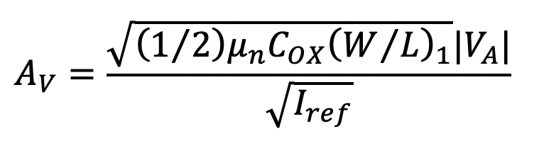
Fig. 5.45: Circuit arrangement illustrating the effect of MOSFET threshold voltage on the switch range of operation.
|
Fig. 5.46: The LTSpice captured circuit schematic for calculating the step response of the NMOS switch arrangement shown in Fig. 5.45 for aspect ratios of 100u/100u and 500u/100u. |


Fig. 5.47: The step response of a NMOS switch arrangement shown in Fig. 5.45 for two different sized MOSFETs.
A single transistor acting as a switch has another serious problem - namely - its limited range of operation, which is caused by its non-zero threshold voltage. To illustrate this limitation, consider the switch arrangement shown in Fig. 5.44. Here a single n-channel MOSFET is connected between the voltage source vI and a load consisting of a 100 kW resistor and a 10-pF capacitor. The n-channel MOSFET is assumed identical to that just described above. Moreover, the gate of this MOSFET is biased at +5 V, intended to turn the switch fully on. The LTSpice schematic capture is provided in Fig. 5.46. Now if we simulate the action of this switch using LTSpice with a 10 V step input beginning at -5 V, then, instead of the voltage at the output following the input in its entirety, we see that the output voltage actually clamps at a level of about 1.85 V as seen in Fig. 5.47. It is easily shown that this clamping limit depends on the threshold voltage of the MOSFET, but it may not be quite so obvious that this clamping limit also depends on the i-v characteristics of the switch. To convince oneself of this, consider increasing the size of the transistor so that its i-v characteristics change. For example, let us increase the width of the MOSFET from 100 𝜇m to 500 𝜇m. On re-running the transient analysis, one finds that the output voltage has similar behavior as in the previous case except that the output voltage clamps at a slightly higher voltages of 2.0 V. This is also shown in Fig. 5.47. The reason for this behavior is because the MOSFET must supply a continuous current to the RC load in order to sustain the output voltage.
|
Fig. 5.48: LTSpice element description for the n-channel or p-channel GaAs MESFET. Also listed is the general form of the associated MESFET model statement. A partial listing of the parameters applicable to the n-channel MESFET is given in Table 5.5.
|
Fig. 5.49: The LTSpice large-signal MESFET model under static conditions.
|


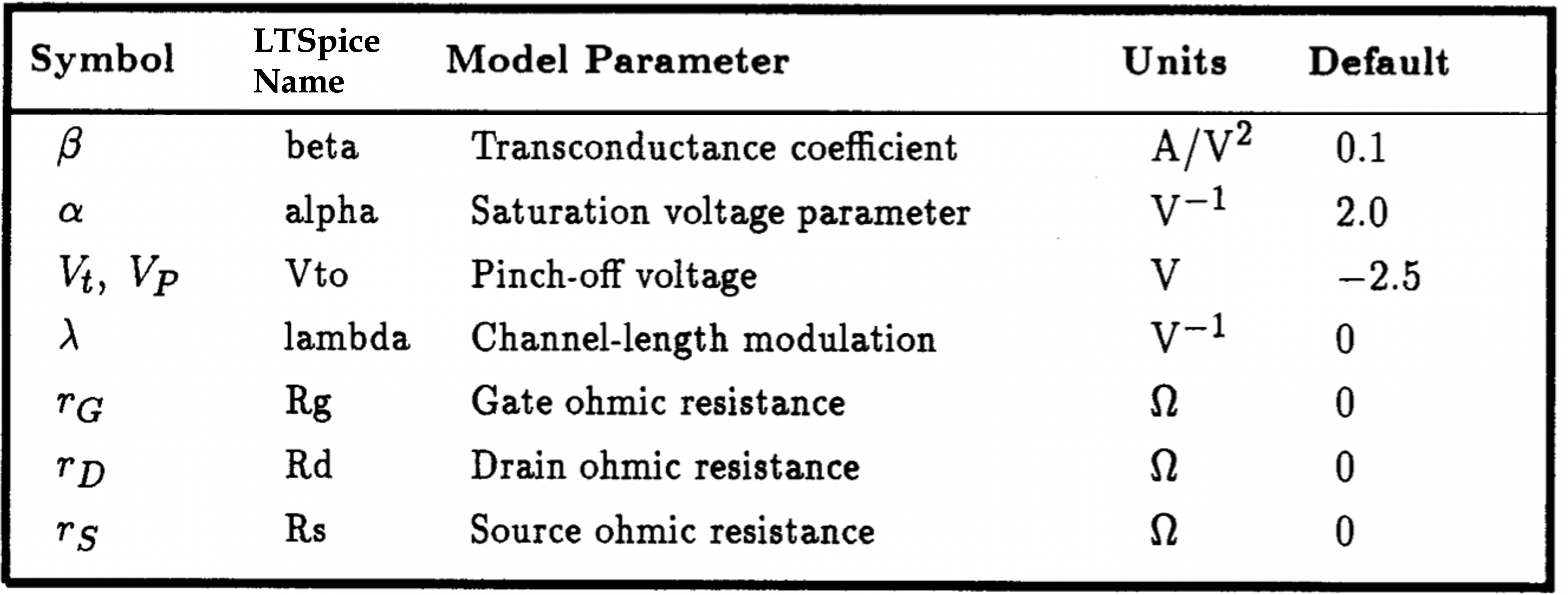
Table. 5.5: A partial listing of the LTSpice parameters for the MESFET model.
|
|
|
Fig. 5.50: Illustrating the dependence of the iD-VDS characteristic of a single n-channel MESFET on the value of a. |

5.7 Describing MESFETs To LTSpice
Built-in models for metal-semiconductor FETs (MESFETs) are available in LTSpice. MESFETs are described to LTSpice in the exact same way as any other semiconductor device is described to LTSpice; that is, using an element statement and a model statement. The device is reference using an element call beginning with the letter Z. The following outlines the syntax of these two statements, including the details of the built-in MESFET model of LTSpice.
5.7.1 MESFET Element Description
MESFETs are described in a LTSpice using an element statement beginning with a unique name prefixed with the letter Z. This is followed by a list of nodes that the drain, gate, and source of the MESFET are connected to. Subsequently, in the next field, a name of a model characterizing the particular MESFET is given - more on this in a moment. The final field of this statement is optional, and its purpose is to allow one to scale the size of the device by declaring the number of MESFETs that are connected in parallel. Unlike a MOSFET, the aspect ratio of the device is not specified. There are other options available as well but are not described here. A summary of the element statement syntax for the n-channel or p-channel MESFET is provided in Fig. 5.48. Included in this list is the corresponding syntax for the MESFET model statement (.MODEL) that must be present whenever a MESFET is made reference to. This statement defines the terminal characteristics of the MESFET by specifying the values of particular parameters in the MESFET model. Parameters not specified in the model statement are assigned default values by LTSpice. Details of this model will be discussed briefly next. An n-channel MESFET is specified using the call words NMF and a p-channel MESFET is referenced using the call words PMF.
5.7.2 MESFET Model Description
As is evident from Fig. 5.48, the model statement for the n-channel MESFET begins with the keyword .MODEL and is followed by the name of the model used by a MESFET element statement, the polarity of the MESFET (i.e., NMF or PMF), and a list of the parameters characterizing the terminal behavior of the MESFET is enclosed between round brackets. The parameters describing the terminal characteristics of the MESFET are quite similar to those used previously to describe the JFET. An additional parameter (a) has been added to properly account for the early saturation phenomenon of the MESFET [Hodges and Jackson, 1983].
The general form of the DC Spice model for an n-channel MESFET is illustrated schematically in Fig. 5.49. The bulk resistance of the drain, gate, and source regions of the MESFET are lumped into three linear resistances rD, rG, and rS, respectively. The DC characteristic of the intrinsic MESFET is determined by the nonlinear dependent current source iD and the two Schottky-barrier diodes. These two Schottky diodes represent the metal semiconductor junctions that define the channel region. The equation describing the drain current for the MESFET model is given below:
(5.16)
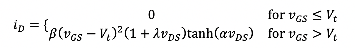
Here the same equation is used to describe both the triode and saturation regions of the device; the distinction between the two is provided by the factor tanh(avDS). This factor also accounts for the early saturation phenomenon observed in MESFETs. See the i-v characteristics in Fig. 5.50 for an n-channel MESFET consisting of 100 transistors connected in parallel having individual device parameters: Vt=-1 V, b=10-4 A/V2, lambda=0.05 V-1, and a taking on values of 0.5, 1.0, and 2.0. The gate-source voltage is assumed to be equal to 0 V. As an extreme limit, the i-v characteristic for a=10^6 is also included. In these equations, b and lambda have the same meaning as in the Spice JFET model. That is, b is the device transconductance parameter, and lambda is the channel-length modulation coefficient.
A partial listing of the parameters associated with the Spice MESFET model under static conditions is given in Table 5.5. Also listed are the associated default values which a parameter assumes if a value is not specified for it on the .MODEL statement. To specify a parameter value one simply writes, for example: beta=20𝜇, Vto=-1V, etc.
5.7.3 Small-Signal MESFET Model
The linear small-signal model of the n-channel MESFET is identical to that seen previously for the JFET in Fig. 5.25(b). It consists of a single voltage-controlled current source having transconductance gm. Here gm is the MESFET transconductance and is related to the DC bias according to the following:
(5.17)
![]()
Likewise, the output conductance gds, which is also equal to 1/ro, is computed according to the following:
(5.18)
|
(a)
(b)
Fig. 5.51: (a) A MESFET amplifier with MESFET load. (b) LTSpice schematic capture with DC sweep command.
|
A Stacked MESFET Amplifier * * Circuit Description * * dc supplies VDD N001 0 10V * input signal Vin IN 0 -0.3V * amplifier circuit Z1 OUT IN 0 n_mesfet 100 Z2 N001 OUT OUT n_mesfet 50 * mesfet model statements (by default, level 1) .model n_mesfet NMF (beta=100u Vto=-1V lambda=0.1) * * Analysis Requests * * calculate DC transfer characteristics .DC Vin -2V 2V 1mV .backanno .end
Fig. 5.52: The LTSpice generated circuit netlist for calculating the DC transfer characteristic of the MESFET amplifier circuit shown in Fig. 5.51.
|


Fig. 5.53: The DC transfer characteristics of the MESFET amplifier shown in Fig. 5.51 as calculated by LTSpice.
5.7.4 A MESFET Biasing Example
As an example of an application of GaAs MESFETs, in Fig. 5.51 we display a simple MESFET amplifier circuit. The lengths of the two devices are assumed to be equal to the minimum value for a particular technology (1 𝜇m in this case). Whereas the width dimensions of B1 and B2 are W1=100 𝜇m and W2=50 𝜇m, respectively. The characteristics of the GaAs process is specified in terms of the electrical parameters of minimum sized devices (i.e., L=1 𝜇m and W=1 𝜇m), and will be assumed to be: Vt=-1 V, b=10-4 A/V2} and 𝜆=0.1 V-1. To determine the parameters of a particular device, it is a simple matter to scale the appropriate parameters of the unit-sized device. Alternatively, we can let LTSpice perform this scaling operation for us. We shall illustrate the latter, since LTSpice is less likely to make a mistake than we are.
Using the device parameters for the minimum-sized device, we can establish the following PSpice model statement for the unit-sized n-channel MESFET:
.model n_mesfet gasfet (beta=0.1m Vto=-1.0V lambda=0.1)
Parameters not specified will, as usual, assume default values.
To account for the different widths of the two transistors, we simply specify on the element statement of each MESFET the ratio of the transistor width to the unit-sized width. In this case, the unit-sized width is 1 𝜇m, so for Z1 with a device width of 100 𝜇m one would specify a scale factor of 100. Of course, this has identical meaning as connecting 100 unit-sized transistors in parallel. Likewise, one would specify a scale factor of 50 for the other transistor. To illustrate, consider the generic element statement for transistor Z1 would be written as
Z1 D G S n_mesfet 100.
With the aid of LTSpice, we would like to determine the DC transfer characteristics of this amplifier. This is easily performed using the LTSpice schematic capture, together with Spice directives, given in Fig. 5.51(b). Here we are sweeping the input voltage level between -2 V to +2 V in 1 mV steps. The input voltage should normally remain negative, otherwise the input metal-semiconductor junction of B1 (the gate-source Schottky diode) becomes forward biased. For demonstration purposes, we are allowing the input voltage to go slightly positive in order to observe the effect of forward biasing this junction.
The resulting DC transfer characteristics of this MESFET amplifier are on display in Fig. 5.52. Here we see that the amplifier has inverter-like characteristics, with its high gain region in the vicinity of a -0.3 V input level. When the input signal level goes more positive than 0.7 V we see that the output voltage begins to rise, corresponding to the fact the input metal-semiconductor junction of the MESFET has become forward biased and that the gate voltage no longer controls the drain-to-source current. Using the transfer function (.TF) command we can determine the voltage gain in the high-gain region of the amplifier. This requires that we bias the input to the amplifier at -0.3 V. Further, we need to change the analysis request from a DC sweep to the following small-signal transfer function command:
.TF V(OUT) Vin
On completion of LTSpice, we find the following small-signal characteristics associated with the MESFET amplifier:
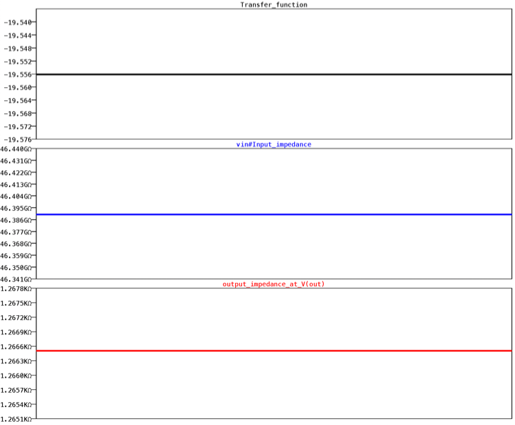
Here we see that the gain in the linear region of the MESFET amplifier is -19.5 V/V, about a factor of 5 times less than the gain available with the simple CMOS amplifier discussed previously in Section 5.6. This result seems to correspond directly with the result that the output resistance for the MESFET amplifier is about five times lower than the output resistance of the CMOS amplifier.
Running a separate dc analysis using the .OP command, results in the following small-signal data:
|
Semiconductor Device Operating Points:
--- MESFETS --- Name: z2 z1 Model: n_mesfet n_mesfet Id: 5.92e-03 5.92e-03 Vgs: 0.00e+00 -3.00e-01 Vds: 5.39e+00 4.61e+00 Gm: 1.05e-02 1.54e-02 Gds: 3.85e-04 4.05e-04 Cgs: 0.00e+00 0.00e+00 Cgd: 0.00e+00 0.00e+00
|
It is re-assuring that when these values are substituted into the formula for the small-signal voltage gain given by AV = - gm,1 (ro1||ro2) we find Av = -19.5 V/V; a result that is very similar results to those computed by LTSpice.
5.8 Chapter Summary
· FETS are described to LTSpice using an element statement and a model statement. The element statement describes the connections that the FET makes to the rest of the network and the name of the model that specifies its terminal behavior. The model statement assigns particular values to internal parameters of the built-in FET model of LTSpice. Parameters whose values are not specified on the model statement are assigned default values.
· LTSpice has built-in models for MOSFETs and JFETs.
· LTSpice has built-in models for MOSFETs and JFETs, and in addition MESFETs.
· Vt0 is positive for enhancement-mode n-channel MOSFETs and depletion-mode p-channel MOSFETs.
· Vt0 is negative for depletion-mode n-channel MOSFETs and enhancement-mode p-channel MOSFETs.
· Vt is negative for both n-channel and p-channel JFETs.
· Vt is negative for an n-channel depletion MESFET and is positive for the n-channel enhancement MESFET.
· A small-signal analysis of an amplifier should always be computed around a known operating point and one that is normally within the linear region of the amplifier. The best way to determine the appropriate operating point is by first performing a DC sweep of the input voltage over the range defined by the power supplies and locating the linear region of the amplifier. The input to the amplifier is then biased inside this region where Spice can compute the small-signal behavior.
5.9 LTSpice Tips
· To investigate the i-v characteristic of a MOSFET subject to different 𝜆 factors, the lambda parameter in a model statement is assigned a variable using the bracket { } notation and a .STEP directive is used to repeat the number of times the DC sweep analysis is performed according to the following:
|
.model nmos_enhancement_mosfet nmos (kp=20u Vto=+2V lambda={lambda_variable}) .STEP param lambda_variable 0 0.05 0.01; * vary lambda_variable from 0 to 0.05 in increments of 0.01 |
· Random number generators are used to model a component whose value is treated as a random variable. There are three types of random number generator available in LTSpice: zero-mean value Gaussian distribution, zero-mean value uniform distribution, and a non-zero mean-value uniform distribution.
+ A zero-mean value Gaussian distributed random variable with standard deviation 𝜎 is called using the function gauss(𝜎).
+ A zero-mean value uniform distributed random variable from -𝜁 to 𝜁 is called using the function flat(𝜁).
+ A component with value 𝜇 that is uniformly distributed from 𝜇*(1-𝛿) to 𝜇*(1+𝛿) is called using the function mc(𝜇,𝜎).
+ All random variable calls must be placed inside brackets, { }.
· To invoke the selection of a new random component for a Spice analysis involving N trials, the following .STEP directive is used:
.STEP PARAM run 1 N 1
where run is just a dummy variable representing the sample iteration.
5.10 Bibliography
A. Vladimirescu and S. Liu, The simulation of MOS integrated circuits using SPICE2, Memorandum no. M80/7, February 1980, Electronics Research Laboratory, University of California, Berkeley.
R.L. Geiger, P. E. Allen and N. R. Strader, VLSI Design Techniques For Analog And Digital Circuits, New York: McGraw-Hill, 1990.
D.A. Hodges and H. Jackson, Analysis and Design of Digital Integrated Circuits, New York: McGraw-Hill, 1983.
5.11 Problems
5.1. Let an n-channel enhancement transistor for which 𝜇COX=50 𝜇A/V2, W=L=25 𝜇m and Vt=2 V be operated with VGS=6 V. Find iD for vDS=2 V using LTSpice. Repeat with vDS=6 V.
5.2. An enhancement PMOS transistor has 𝜇COX=40 𝜇A/V2, L=25 𝜇m, W=50 𝜇m, Vt=-1.5 V, and 𝜆= 0.02 V-1. The gate is connected to ground and the source to +5 V. Find the drain current using LTSpice for (a) vD=4 V, (b) vD=+1.5 V, (c) vD=0 V, and (d) vD=-5 V.
5.3. A depletion-type n-channel MOSFET with 𝜇COX=4 mA/V2 and Vt=-3 V has its source and gate grounded. With the aid of LTSpice, find the region of operation and the drain current for (a) vD=0.1 V, (b) vD=1 V, (c) vD=3 V, and (d) vD=5 V. How do these results compare with hand analysis? Repeat with lambda = 0.05 V-1.
5.4. A depletion-type PMOS transistor has IDSS=8.8 mA, Vt=+2.2 V and lambda = 0.04 V-1. The source is connected to ground, the gate is connected to -2 V and a 2-mA current is pulled from the drain, using LTSpice determine the source-drain voltage. Assume that the width of the MOSFET is twice that of its length. Compare your results with a hand analysis.
5.5. Design the circuit of Fig. 5.3 to establish a drain current of 1 mA and a drain voltage of 0 V. The MOSFET has Vt=2 V, 𝜇COX=20 𝜇A/V2, L= 10 𝜇m and W=400 𝜇m. Confirm your design using LTSpice. How much does the drain current change (in percent) when the effect of channel-length modulation is included in the LTSpice model of the MOSFET (assume lambda = 0.04 V-1)?
5.6. Using LTSpice as a curve tracer, plot the iD - vDS characteristics of an enhancement-mode n-channel MOSFET having 𝜇COX=50 𝜇A/V2, L=25 𝜇m, W=50 𝜇m, Vt=+1.5 V, and 𝜆=0.04 V-1. Provide curves for VGS=1, 2, 3, 4 and 5 volts. Show the characteristics for vDS up to 10 V.
5.7. Using LTSpice as a curve tracer, plot the iD - vDS characteristics of a depletion-mode p-channel MOSFET having 𝜇COX=50 𝜇A/V2, L=25 𝜇m, W=50 𝜇m, Vt=+1.2 V, and 𝜆= 0.04 V-1. Provide curves for VGS=-1, -2, -3, -4 and -5 volts. Show the characteristics for vDS from 0 to -10 V.
5.8. Consider an n-channel JFET with IDSS=4 mA and VP=-2 V. If the source is grounded and a -1 V dc voltage source is applied to the gate, using LTSpice find the drain current that corresponds to the minimum drain voltage that results in pinch-off operation.
5.9. For a JFET having VP=-2 V and IDSS= 8 mA operating at VGS=-1 V and a very small vDS, with the aid of LTSpice, determine the value of rDS.
5.10. Using LTSpice as a curve tracer, plot the iD - vDS characteristics of an n-channel JFET with IDSS=8 mA and VP=-4 V and lambda=0.01V-1. Provide curves for VGS=-5, -4, -3, -2 and 0 volts. Show the characteristics for vDS up to 10 V.
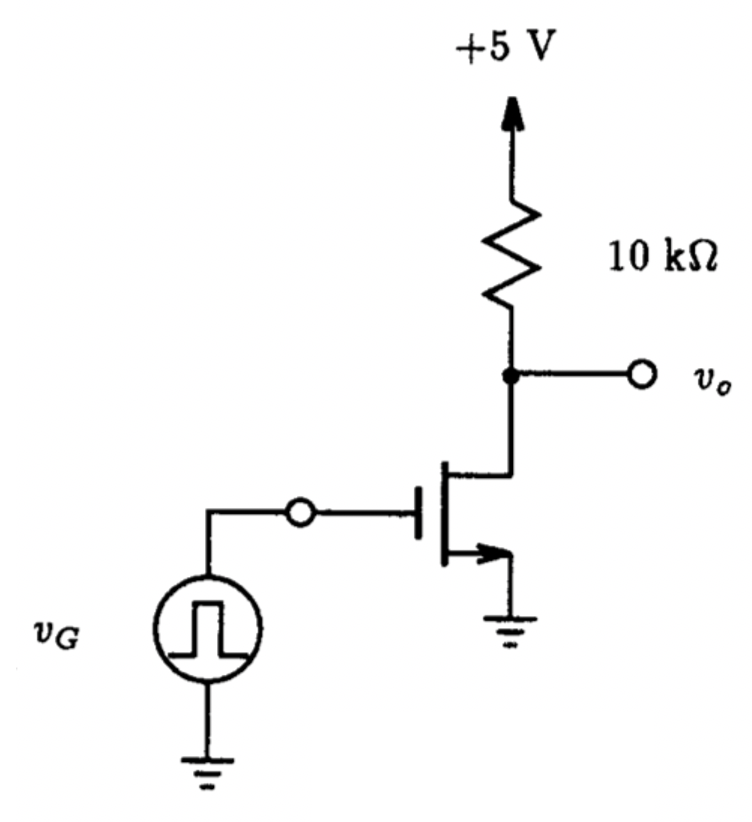
Fig. P5.11
5.11. The NMOS transistor in the circuit of Fig. P5.11 has Vt=1 V, 𝜇COX= 1 mA/V2, and 𝜆=0.02 V-1. If vG is a pulse with 0 and 5 V levels and having a 1 ms pulse width, simulate the circuit using LTSpice and determine the pulse signal that appears at the output.
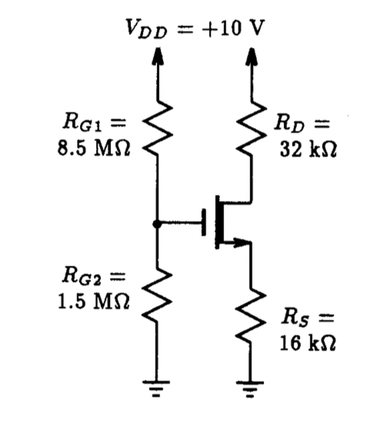
Fig. P5.12
5.12. Simulate the circuit in Fig. P5.12 to determine the drain current and the drain voltage. Assume that the depletion MOSFET has Vt=-1 V, 𝜇COX= 1 mA/V2, and lambda=0.03 V-1. If K of the MOSFET increases by a factor of 2, determine the new level of drain current and drain voltage. Compare this to the previous case and note whether the biasing scheme is very effective.
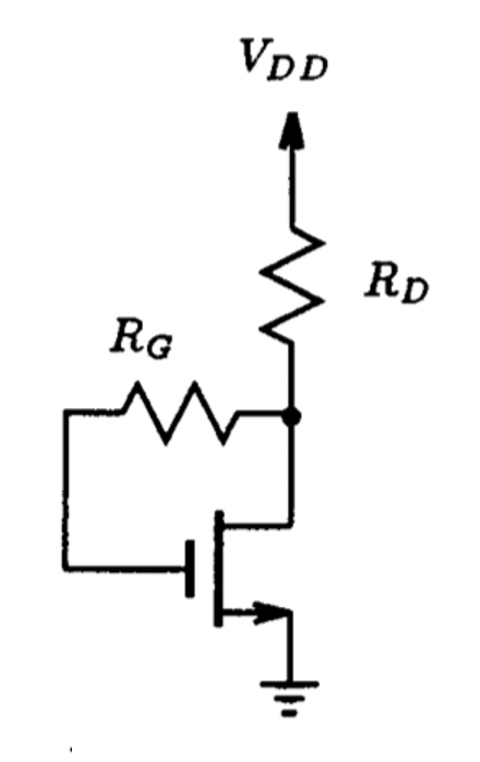
Fig. P5.13
5.13. A MOSFET having 𝜇COX= 2 mA/V2 and Vt=1 V operates in a feedback bias arrangement such as that shown in Fig. P5.13, from a 10 V supply with RD=8 kW and RG=10 MW. What value of ID results? If the FET is replaced by another with (a) 𝜇COX= 1 mA/V2 and Vt=1 V, and (b) 𝜇COX= 2 mA/V2 and Vt=2 V, what percentage change in ID results?
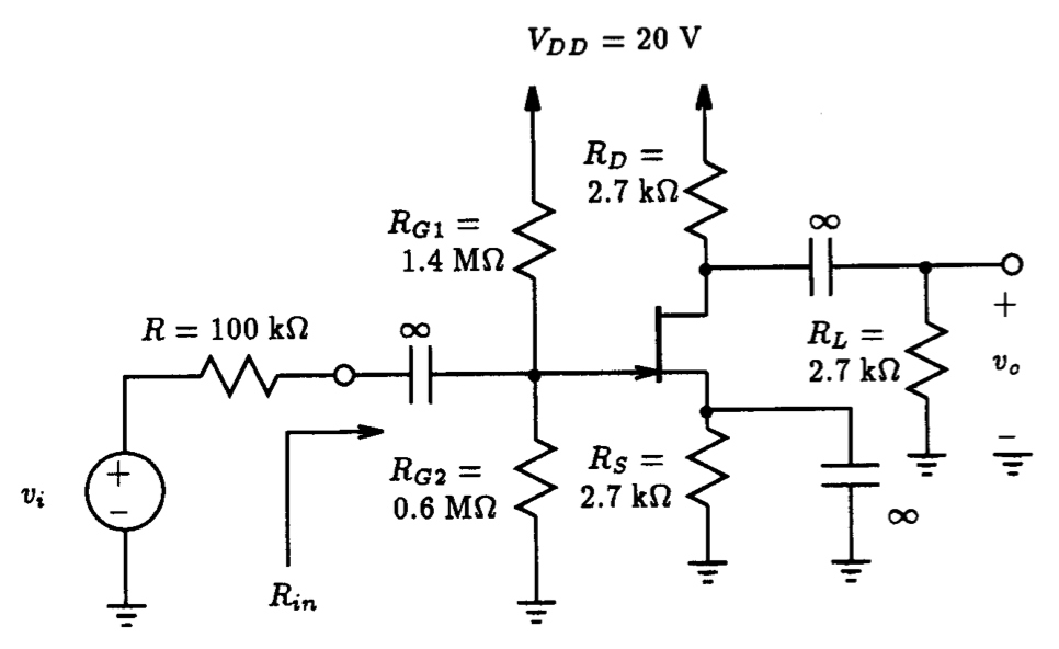
Fig. P5.14
5.14. The JFET in the amplifier circuit in Fig. P5.14 has VP=-4 V, IDSS=12 mA and lambda=0.003 V-1. Using LTSpice, answer the following:
(a) Determine the dc bias quantities V_G, ID, VGS, and vD associated with the JFET.
(b) Determine the overall voltage gain vo/vi and input resistance Rin.
Fig. P5.15
5.15. In the circuit of Fig. P5.15 all devices are matched and assumed to have the following parameters: 𝜇COX=50 𝜇A/V2, W=L=25 𝜇m and Vt=2 V. Using Spice, plot the transfer characteristics vO vs. vI between VDD and ground. What is the small-signal voltage gain in the linear region of this amplifier? What is the corresponding output resistance?
Fig. P5.16
5.16. A CMOS switch for which 𝜇COX= 50 𝜇A/V2, g=0.3 V1/2 and |Vt0|=2 V is placed in the circuit setup shown in Fig. P5.16 for measuring its on-resistance. Sweep the input voltage signal vI from -5 V to +5 V using LTSpice and determine the resistance of the switch over this range of signals. Compare these results to those obtain from a switch consisting of a single n-channel MOSFET.
5.17. A CMOS switch is used to connect a sinusoidal source of 0.1 sin(2p 103t) to a load consisting of a 10 kW resistor and a 5 pF capacitor. If the control terminals of the switch are driven by complementary signals of ±5 V at a frequency of 10 kHz, simulate the transient behavior of the switch using LTSpice. Assume that the model parameters of the NMOS and PMOS devices are 𝜇nCOX=20 A/V2, 𝜇pCOX=10 A/V2, |Vt0|=1 V, 𝛾=0.3 V1/2, Ln=Lp=5 𝜇m, Wn=15 𝜇m, and Wp=30 𝜇m.
5.18. Using LTSpice as a curve tracer, plot the iD - vDS characteristics of an n-channel MESFET with b=10-4 A/V2, Vt=-1 V, IS=10-15 A and lambda=0.1 V-1. Provide curves for VGS=-5, -4, -3, -2 and 0 volts. Show the characteristics for vDS up to 10 V.
5.19. The n-channel MESFET in the circuit of Fig. 5.50 has Vt=-1 V, b=0.1 mA/V2, and 𝜆=0.1 V-1. If vi is a pulse with -5 and 0 V levels of 1 𝜇s pulse width, simulate the circuit using LTSpice and plot the pulse signal that appears at the output.