Chapter 7
Amplifier Stages with Large Current Drive Capability
Gordon W. Roberts
Department of Electrical & Computer Engineering, McGill University
This chapter is concerned with the study of amplifier stages that provide large current drive capability. Such amplifiers are used to interface other amplifiers to small impedance loads such as speakers (4 – 16 Ω) or headphones (32 – 120 Ω), motor drives or RF transmitters. They are used as the final block in an amplifier chain and are often referred to as output stages. Output stages are used to supply large amounts of power to a load over a desired voltage range with very little signal distortion and with high power conversion efficiency. In this chapter we shall demonstrate how one utilizes LTSpice to compute the various performance measures of an output stage. This will include such measures as current drive, power efficiency and harmonic distortion. In addition, we shall also investigate the role of short-circuit protection circuits that are commonly incorporated into the circuit of an output stage.
7.1 Emitter-Follower or Class A Output Stage
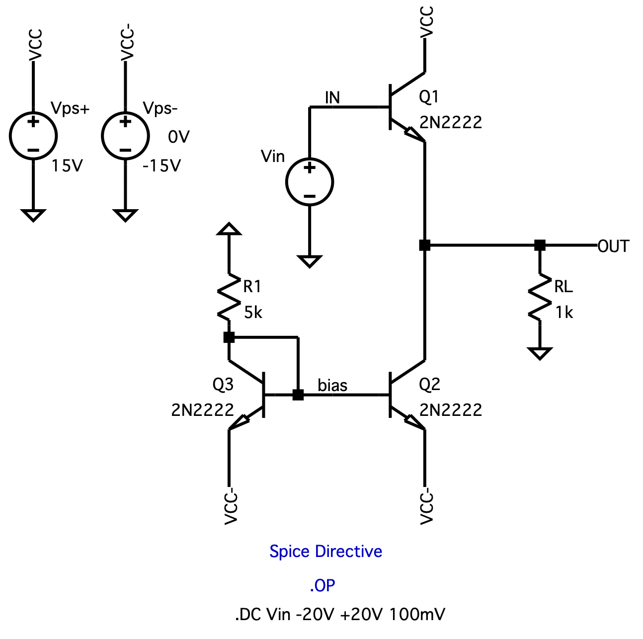
In Fig. 7.1 a display of an emitter-follower output stage biased with a constant current source of Ibias » (15-0.7)/5k = 2.86 mA realized by transistors Q2, Q3 and resistor R is shown. The output terminal of this stage is connected to a load resistance of 1 kW. With the aid of LTSpice, we would like to determine the transfer characteristic of the emitter-follower assuming that each transistor is modeled after the widely available commercial 2N2222 npn transistor. The LTSpice input listing of the emitter-follower circuit is seen listed in Fig. 7.2. A DC sweep of the input voltage source is requested to be performed between -20 V and +20 V. with 100 mV steps using the following Spice directive:
.DC Vin -20V +20V 100mV
Although this particular voltage sweep extends beyond the power supply limits of the output stage, it is intended to highlight the saturation limits of the emitter-follower circuit.
On completion of this analysis, the large-signal input-voltage-to-output-voltage transfer curve for the emitter follower is shown in Fig. 7.3(a). As is evident from these results, the output voltage saturates at -3.25 V for inputs below -2.7 V, and saturates at +14.9 V for input levels beyond +15.6 V. This stage also exhibits an input offset voltage of +0.67 V. The slope of the transfer characteristic within the linear region of operation is very nearly unity (i.e., 0.995 V/V). In addition, a plot of the output current as a function of the input voltage is shown in Fig. 7.3(b). Here one sees the load current ranges between -3 mA to 15 mA inside the saturation limits. Consequently, the DC load power V(OUT) × I(RL) as a function of the input voltage is displayed in Fig. 7.3(c). As can be seen here the DC load power ranges from 0 to 220 mW over its linear operation. This power, of course, is supplied by the power supplies via the output stage.
An important drawback of this output stage is that the output cannot swing equally in both directions about a 0 V output level, as the lower saturation limit of IbiasRL is set by an external current source Ibias. It is interesting to note that the lower saturation limit of the output voltage is somewhat greater than that predicted by the simple equation IbiasRL. Specifically, according to this simple expression, the lower saturation limit should be -2.86 mA x 1k Ω = -2.86 V, instead of the simulation result of -3.25 V. The reason for this deviation from the simple theory is due to the fact that the output current of the current source Q2 varies with output voltage. This is confirmed by the plot of the collector current of Q2 versus the output voltage vout shown in Fig. 7.4. This was found by displaying the collector current Q2 as a function of the output voltage vout through the appropriate selection of the circuit variable and changing the x-axis display to Vout instead of Vin. Notice that at an output voltage of 0 V, the collector current of Q2 equals 3.23 mA and increases with increased output voltages. This is somewhat higher than the initial bias current of 2.86 mA.
|
|
* A Class A Output Stage
** Circuit Description ** * power supplies Vps+ VCC 0 15V Vps- VCC- 0 -15V * input source Vin IN 0 0V * main circuit Q1 VCC IN OUT 0 2N2222 Q2 OUT bias VCC- 0 2N2222 Q3 bias bias VCC- 0 2N2222 R1 0 bias 5k RL OUT 0 1k * transistor model statement form library .lib /Users/roberts/Library/Application Support/LTspice/lib/cmp/standard.bjt * Spice Directives .OP .DC Vin -20V +20V 100mV * .backanno .end |
|
Fig. 7.1: An emitter-follower output stage with current-source bias captured by LTSpice.
|
Fig. 7.2: The Spice input file for computing the transfer characteristics of the emitter-follower output stage shown in Fig. 7.1. |
|
(a) |
(b) |
|
(c) |
|
|
Fig. 7.3: The transfer characteristics of the emitter-follower circuit shown in Fig. 7.1. (a) input voltage – output voltage transfer characteristic, (b) input voltage – load current transfer characteristic, and (c) DC output power transfer characteristic. |
|


|
|
|
Fig. 7.4: The dependence of the collector current of Q2 on the output voltage vOUT.
|

To better understand the behavior of the voltage-follower output stage, let us consider applying several sine-wave signals of 1 kHz frequency having various amplitudes to the input of the circuit. Specifically, we shall use amplitudes of 1 V, 2.7 V and 10 V. In this way we can visualize the expected output signals from the emitter-follower circuit as one would see in the laboratory using a function generator and an oscilloscope. According to the transfer characteristic of the emitter-follower circuit shown in Fig. 7.3, the 1 V sinewave and the 2.7 V sinewave signal centered on an input DC value of 0 V should pass undistorted (although, the 2.7 V signal should just barely pass undistorted). On the other hand, the 10 V signal should become clipped on the negative portion of the output waveform. To see this with LTSpice, the input signal is modified by editing the input voltage source according to
Vi 3 0 sin (0V 1V 1kHz)
Similar statements can be written for the other two input levels, although the easiest approach is to use the .STEP directive and assign the input amplitude as an external parameter using red colour letters according to the following:
Vi 3 0 sin (0V {Amp} 1kHz)
.STEP PARAM Amp LIST 1V, 2.7V, 10V
Finally, a .TRAN Spice directive is specified to observe three cycles of the 1 kHz signal according to
|
.TRAN 10us 3ms 0ms 10us
|
Here one hundred points per period of the output waveform will be collected and plotted.
|
|
|
|
Fig. 7.5: The input and output voltage waveform of the voltage-follower circuit of Fig. 7.1 for three different input levels: 1 V, 2.7 V and 10 V. Excessive voltage clipping occurs on the negative portion of the output voltage waveform (bottom plot) corresponding to an input amplitude of 10 V.
|
Fig. 7.6: Several waveforms associated with the emitter-follower circuit of Fig. 7.1 when excited by a 2.7 V, 1 kHz sinusoidal signal. The top graph displays the voltage across the load resistance, the next graph displays the collector-emitter voltage of Q1, the third graph from the top displays the collector current of Q1, and the bottom graph displays the instantaneous power dissipated by Q1.
|


On completion of the LTSpice analysis, the input and output of the emitter-follower for the three different input signals are shown plotted in Fig. 7.5. These results confirm that for sine-wave inputs less than 2.7 V, the output waveform does not reveal any obvious distortion. On the other hand, for an input sinewave of 10 V peak, the negative portion of the output sinewave is clipped at a level of about -3.25 V.
Other waveforms associated with the emitter-follower as calculated by LTSpice are shown in Fig. 7.6. The input to this circuit is a 2.7 V sine-wave signal of 1 kHz frequency (the largest input signal that can be applied to the emitter-follower circuit before distortion sets in). The top graph shows the voltage waveform that appears across the load resistance. The output signal is sinusoidal with a peak value of 2.57 V riding on a DC level of -0.690 V. The second and third graph from the top display both the collector-emitter voltage and the collector current of transistor Q1, respectively. Both of these waveforms appear sinusoidal with amplitudes of 2.57 V and 2.63 mA, respectively. The average value of the voltage waveform appearing between the collector and emitter terminals is 15.68 V. Similarly, the average value of the collector current is 2.52 mA. The bottom-most graph displays the instantaneous power dissipated by Q1. This waveform was obtained by multiplying together the collector current and collector-emitter voltage of Q1 using Probe. The peak value associated with this waveform is 68.4 mW and its average value is about 40 mW.
|
|
* A Class B Output Stage
** Circuit Description ** * power supplies Vps+ VCC 0 23V Vps- VCC- 0 -23V * input source Vin IN 0 SINE(0V 1V 1000) * main circuit Q1 VCC IN OUT 0 2N3055 Q2 VCC- IN OUT 0 D45H11 RL OUT 0 8 * BJT Transistor Models .model NA51 NPN (Is=10f Xti=3 Eg=1.11 Vaf=100 Bf=100 Ise=0 Ne=1.5 Ikf=0 + Nk=.5 Xtb=1.5 Br=1 Isc=0 Nc=2 Ikr=0 Rc=0 Cjc=76.97p Mjc=.2072 + Vjc=.75 Fc=.5 Cje=5p Mje=.3333 Vje=.75 Tr=10n Tf=1n Itf=1 Xtf=0 + Vtf=10) .model NA52 PNP (Is=10f Xti=3 Eg=1.11 Vaf=100 Bf=100 Ise=0 Ne=1.5 Ikf=0 + Nk=.5 Xtb=1.5 Br=1 Isc=0 Nc=2 Ikr=0 Rc=0 Cjc=112.6p Mjc=.1875 + Vjc=.75 Fc=.5 Cje=5p Mje=.3333 Vje=.75 Tr=10n Tf=1n Itf=1 Xtf=0 + Vtf=10) * Spice Directive * .OP .DC Vin -10V +10V 100mV *.TRAN 10us 3ms 0ms 10us *.FOUR 1kHz V(OUT) .backanno .end |
|
Fig. 7.7: Schematic circuit captured by LTSpice of a Class B output stage using National Semiconductor complementary power transistors NA51 and NA52.
|
Fig. 7.8: The Spice input file for computing the transient response of the class B output stage shown in Fig. 7.7. A 17.9 V, 1 kHz sinusoid is applied to the input.
|

|
(a) |
(b) |
|
(c) |
|
|
Fig. 7.9: The input-output transfer characteristics of a class B output stage: (a) input voltage – output voltage transfer characteristic, (b) input voltage – load current transfer characteristic, and (c) DC output power transfer characteristic. |
|


|
|
|
|
Fig. 7.10: Illustrating the input-output effect of the dead-band region on a 1-V, 1 kHz input sinusoidal signal riding on two different DC levels: (a) 0 V, and (b) 5 V.
|
|


7.2 Class B Output Stage
In Fig. 7.7 we display a class B output stage loaded by an 8 W resistor and driven by voltage source Vi. It consists of a pair of complementary transistors assumed to have similar characteristics. This output stage is noted for its relatively high-power conversion efficiency (at most, 78.5%), and its large crossover distortion. In the following we shall investigate these two attributes of the class B output stage using LTSpice and assuming that the transistors are modeled after National Semiconductor's complementary NA51 and NA52 transistors. The corresponding netlist for this circuit is provided in Fig. 7.8.
Transfer Characteristic and Distorted Output Signal
The large-signal transfer characteristic of the class B amplifier was derived by sweeping the input voltage Vin from -10 V to +10 V using the following .DC Spice directive:
.DC Vi -10V +10V 100mV
The results are on display in Fig. 7.9 for the input-voltage output-voltage transfer curve, the input-voltage load-current transfer curve and the input-voltage DC load-power transfer curve. Unlike the straight-line transfer curve for the class A amplifier shown in Fig. 7.3, the class B amplifier experiences a dead-band region in the vicinity of the input bounded by -0.72 V to +0.72 V. No such dead-band region is evident in the transfer curve for the class A amplifier of Fig. 7.3. This is an important distinction. It is also apparent form these curves that the Class B amplifier is capable of deliver a very large current to the load without the use of any current source biasing.
To better understand the effect of the dead-band region on the operation of the class B amplifier, let us consider applying a 1 V, 1 kHz sine-wave signal riding on a 0 V DC level to the input of the class B amplifier and perform a transient analysis using the following Spice directive:
|
.TRAN 10us 3ms 0ms 10us
|
The results of this analysis are shown in Fig. 7.10(a). As is evident, the output signal is a highly distorted version of the input signal. It is interesting to note that if the DC level of the 1 V, 1 kHz sinewave is changed to 5 V using the following source statement,
Vi 3 0 sin (5V 1V 1kHz),
then the output signal experiences little or no visible distortion effects as seen in the plot in Fig. 7.10(b). Thus, depending on how the input signal interact with the amplifier transfer characteristic, the distortion may or may not be visible in the output signal.
|
|
|
Table 9.1: The general syntax of the Fourier Analysis command in Spice. |

A Measure of Linearity – Total Harmonic Distortion
Although the dead-band effect is very visible in the amplifier transfer characteristic, one prefers to quantify the effect of this dead-band region using a Fourier Series measure that decomposed the output signal in terms of its harmonic components when subjected to a sinusoidal input signal. LTSpice provides this analysis capability through the Fourier Analysis command. This command simply decomposes a waveform generated through a transient analysis into its Fourier series components. This includes the fundamental, a DC component, and the next eight harmonics. LTSpice will also compute the total harmonic distortion (THD) of the waveform.
The syntax of the .FOUR command is described in Table 9.1. The Spice directive .FOUR specifies that a Fourier series decomposition is to be performed on each variable indicated in the variable list found after the field specifying the specified frequency of the fundamental, i.e., fundamental_frequency. It is important to note that the Fourier analysis performed by LTSpice is not done on the entire waveform computed by the transient analysis. Instead, it is performed only on the waveform defined between its end time and one period of the fundamental back from this end time (i.e., 1/fundamental_frequency seconds). This implies that the transient analysis used in conjunction with a Fourier analysis must be at least 1/fundamental_frequency seconds long. The results of the Fourier analysis command (.FOUR) appear in table format in the SPICE Error Log file. One must open this file using a text editor and observe the results.
Returning to the schematic circuit of Fig. 7.7, we can add a Fourier analysis command and compute the total harmonic distortion (THD) contained in the output voltage waveform. This is achieved simply by adding the following .FOUR command, combined with the 1 V, 1 kHz input sinusoidal signal to the LTSpice circuit description:
Vi 3 0 sin (0V 1V 1kHz)
.FOUR 1kHz V(OUT)
The results of the Fourier analysis found in the Spice Error Log File is as follows:
|
Fourier components of V(out)
DC component:-6.00832e-06
Harmonic Frequency Fourier Normalized Phase Normalized Number [Hz] Component Component [degree] Phase [deg] 1 1.000e+3 1.644e-1 1.000e+0 0.00° 0.00° 2 2.000e+3 2.853e-6 1.736e-5 60.53° 60.53° 3 3.000e+3 9.010e-2 5.482e-1 -180.00° -180.00° 4 4.000e+3 9.464e-6 5.757e-5 77.36° 77.36° 5 5.000e+3 1.486e-2 9.043e-2 -0.02° -0.02° 6 6.000e+3 6.255e-6 3.806e-5 -100.54° -100.54° 7 7.000e+3 1.039e-2 6.323e-2 0.01° 0.00° 8 8.000e+3 3.658e-6 2.225e-5 -138.16° -138.16° 9 9.000e+3 2.692e-3 1.637e-2 179.95° 179.95°
Total Harmonic Distortion: 55.939316%(55.976595%)
|
As is evident from above, the output voltage from the class B output stage is rich in odd-order harmonics, resulting in a rather an extremely high THD measure of 55.9% (or 55.97% by a second metric evaluation). If the input amplitude is increased to 17.7 V and continues to ride on a 0 V DC signal level, then the results of the Fourier analysis leads to a much lower THD measure of 2.57% as listed in the Spice Error log file:
|
Fourier components of V(out)
DC component:0.000566348
Harmonic Frequency Fourier Normalized Phase Normalized Number [Hz] Component Component [degree] Phase [deg] 1 1.000e+3 1.659e+1 1.000e+0 -0.01° 0.00° 2 2.000e+3 1.128e-3 6.800e-5 95.25° 95.26° 3 3.000e+3 3.374e-1 2.034e-2 -179.44° -179.43° 4 4.000e+3 1.114e-3 6.716e-5 100.49° 100.50° 5 5.000e+3 1.959e-1 1.181e-2 -179.08° -179.07° 6 6.000e+3 1.092e-3 6.583e-5 105.68° 105.69° 7 7.000e+3 1.356e-1 8.176e-3 -178.74° -178.73° 8 8.000e+3 1.063e-3 6.408e-5 110.78° 110.79° 9 9.000e+3 1.021e-1 6.157e-3 -178.46° -178.45°
Total Harmonic Distortion: 2.565344%(2.724857%) |
|
|
This result should not be too surprising as the dead-band effect introduces the same amount of distortion energy for input sinusoidal signals with an amplitude larger than 0.7 V. Thus, the larger the input amplitude, the smaller the ratio of the dead-band distortion to signal energy. This behavior is generally true for most circuits when operating well with the saturation levels of the amplifier.
Generally, the distortion behavior of a class B output stage is much poorer than that which can be achieved with an emitter-follower circuit with the same input voltage level. To demonstrate this, let us return to the emitter-follower example of the previous section and compute its harmonic content when excited by a 17.7 V, 1 kHz sinusoidal signal. Recall from Section 7.1 that the emitter-follower circuit given there could only handle input signals with peak values less than 2.7 V. Therefore, let us increase the load resistor from 1 kW to 5 kW and the level of the two power supplies to ±23 V. This will increase the range of input signals that can be applied to the input of this amplifier before the output becomes distorted. (Computing the transfer characteristic of this revised voltage-follower circuit using LTSpice indicates that the linear region of this amplifier is between -21.4 V and +23 V).
The results of the Fourier analysis as computed by LTSpice for the voltage-follower circuit are as follows:
|
Fourier components of V(out)
DC component:-0.692139
Harmonic Frequency Fourier Normalized Phase Normalized Number [Hz] Component Component [degree] Phase [deg] 1 1.000e+3 1.763e+1 1.000e+0 0.00° 0.00° 2 2.000e+3 1.728e-3 9.796e-5 -99.91° -99.91° 3 3.000e+3 7.515e-4 4.262e-5 -13.46° -13.46° 4 4.000e+3 1.658e-3 9.404e-5 98.01° 98.01° 5 5.000e+3 1.662e-3 9.427e-5 -167.73° -167.73° 6 6.000e+3 9.110e-4 5.166e-5 -84.74° -84.74° 7 7.000e+3 1.704e-4 9.661e-6 -48.71° -48.71° 8 8.000e+3 6.333e-4 3.591e-5 -73.68° -73.68° 9 9.000e+3 8.093e-4 4.589e-5 15.96° 15.96°
Total Harmonic Distortion: 0.018789%(0.049113%) |
Here we see that the THD for the emitter-follower circuit is 0.018%. This is obviously much less than that seen for the class B stage above at 2.57%.
|
|
Fig. 7.12: The voltage, current, and instantaneous power supplied by the positive voltage supply (+VCC). The upper graph displays the voltage generated by +VCC, the middle graph displays its current waveform, and the lower graph displays the instantaneous power supplied to the rest of the circuit.
|
|
Fig. 7.11: Several waveforms associated with the class B output stage shown in Fig. 7.7 when excited by a 0-V DC, 17.9 V, 1 kHz sinusoidal signal. The upper graph displays the voltage across the load resistance, the middle graph displays the load current, and the lower graph displays the instantaneous power dissipated by the load.
|
|


Power Conversion Efficiency
With a 17.7 V, 1 kHz sinusoidal signal applied to the input of the output stage shown in Fig. 7.7, we would like to determine the average power supplied by the two 23 V power supplies (PS), the average power provided to the load resistance (PL) and the power conversion efficiency (i.e., 𝜂= PL/PS). In addition, we would also like to determine the power that each transistor must dissipate. Using the same LTSpice circuit setup that was used previously, the output voltage, load current and instantaneous load power can be determined as shown in Fig. 7.11. The upper-most graph displays the voltage appearing across the load having a peak amplitude of 16.82 V. The middle curve displays the load current having a peak amplitude of 2.10 A. Notice that both the voltage and current waveforms exhibit a small crossover distortion, as explained in the previous section. The bottom graph of Fig. 7.11 displays the instantaneous power dissipated by the load as computed by the built-in computational facilities of the waveform viewer. The instantaneous power dissipated by the load resistor is computed according to V(out) x I(Rl). The average value of any of these waveforms can be obtained directly from the waveform viewer by moving the mouse over the waveform label at the top of each graph, hold down the control key, then left click the mouse button. For instance, the average of the instantaneous load power V(out)*I(Rl) is found to be 17.211 W, as demonstrated in Fig. 7.12.
|
|
|
|
Fig. 7.13: The voltage, current, and instantaneous power supplied by the positive voltage supply (+VCC). The upper graph displays the voltage generated by +VCC, the middle graph displays its current waveform, and the lower graph displays the instantaneous power supplied to the rest of the circuit. Also, provided is the average power supplied by +VCC.
|
Fig. 7.14: Waveforms of the voltage across, the current through, and the power dissipated in, the pnp transistor QP of the output stage shown in Fig. 7.7.
|


The voltage and current waveforms supplied by the positive voltage supply +VCC are shown in the upper two graphs of Fig. 7.13. Shown in the lower-most graph is the instantaneous power supplied by +VCC. Similar waveforms are found for the negative power supply -VCC except that current is supplied to the output stage in complementary time slots. The average power supplied by either +VCC or -VCC is found to be approximately 14.8 W, for a total supply power (PS) of 29.6 W. The power conversion efficiency is then computed to be 𝜂=PL/PS=17.2/29.6 x 100% = 58.1%.
Another important quantity of concern in the design of an output stage is the amount of power dissipated by the two complementary transistors Q1 and Q2. Figure 7.14 shows plots of the voltage, current, and power waveforms associated with transistor Q2. Similar waveforms apply for Q1. Both the voltage and current waveforms appear as expected. That is, the voltage waveform is sinusoid and the current waveform is a half-wave sinusoid. However, the instantaneous power waveform shown in the bottom-most graph of Fig. 7.14 has a rather strange shape. It appears periodic but is nonsinusoidal - almost pulse-like (less a few higher-order harmonic components). The reason for this is that the two transistors are being driven quite hard, and, although not apparent in the corresponding voltage and current waveforms seen above, some distortion is present and is manifesting itself very clearly in the instantaneous power waveform. The average power dissipated by transistor Q2 is seen to be approximately 6.3 W. Likewise, for transistor Q1.
It is reassuring to confirm that the average power supplied by the two power supplies of 29.6 W approximately equals the sum of the power dissipated by the output stage of 12.6 W and that dissipated by the load of 17.2 W.
|
Table 9.2: The various power terms associated with the class B output stage shown Fig. 7.7 as computed by hand and LTSpice analysis. The rightmost column presents the relative error (in percent) between the values predicted by hand and LTSpice.
|
To compare the above results found through an LTSpice analysis with those calculated by a hand analysis, Table 9.2 was created for easy viewing. The accuracy of the hand calculated results as compared to those computed by LTSpice is also given as a relative error expressed in percent. As is evident, the hand calculated agree quite well with no more than a 5.8% relative error.
|
|
Fig. 7.16: An analog behavior model of a current source: (a) a piecewise linear representation of the current source transfer characteristic, and (b) LTSpice VCCS model description using a piecewise linear table description statement.
|
|
Fig. 7.15: A class AB output stage utilizing diode-connected transistors biased with an ideal current source.
|
|


|
|
* Class AB Output Stage
** Circuit Description ** * power supplies & current sources Vps+ VCC 0 23V Vps- VCC- 0 -23V Gbias VCC N001 VCC N001 table(0V 0mA, 1.999V 0mA, 2V 3mA, 23V 3mA) * input signal source Vin IN 0 SINE(0V 10V 1000) * VBB biasing circuit Q3 N001 N001 N002 0 2N2222 Q4 N002 N002 IN 0 2N2222 * output buffer Q1 VCC N001 OUT 0 NA51 Q2 VCC- IN OUT 0 NA52 * load resistance RL OUT 0 100 * transistor models * pull 2N2222 models from LTSpice library .lib /Users/roberts/Library/Application Support/LTspice/lib/cmp/standard.bjt * complementary power transistors .model NA51 NPN (Is=10f Xti=3 Eg=1.11 Vaf=100 Bf=100 Ise=0 Ne=1.5 Ikf=0 + Nk=.5 Xtb=1.5 Br=1 Isc=0 Nc=2 Ikr=0 Rc=0 Cjc=76.97p Mjc=.2072 + Vjc=.75 Fc=.5 Cje=5p Mje=.3333 Vje=.75 Tr=10n Tf=1n Itf=1 Xtf=0 + Vtf=10) .model NA52 PNP (Is=10f Xti=3 Eg=1.11 Vaf=100 Bf=100 Ise=0 Ne=1.5 Ikf=0 + Nk=.5 Xtb=1.5 Br=1 Isc=0 Nc=2 Ikr=0 Rc=0 Cjc=112.6p Mjc=.1875 + Vjc=.75 Fc=.5 Cje=5p Mje=.3333 Vje=.75 Tr=10n Tf=1n Itf=1 Xtf=0 + Vtf=10) * Spice Directives * .OP .DC Vin -25V +25V 100mV * .TRAN 10us 3ms 0ms 10us *.FOUR 1kHz V(OUT) .backanno .end |
|
Fig. 7.17: A class AB output stage utilizing a biasing current source with a piecewise linear transfer characteristic representation.
|
Fig. 7.18: The Spice netlist file for computing the transfer curve and transient response of the class AB output stage shown in Fig. 7.17. A 10 V, 1 kHz sinusoid is applied to the input.
|

|
|
|
|
Fig. 7.19: The top graph shows the input-output transfer characteristics of a class AB output stage for ideal and actual current source biasing. The bottom graph plots the derivative of the output voltage (actual current source biasing) as a function of the input voltage Vin. Here a small change in the voltage gain occurs around Vin=0 V. |
Fig. 7.20: Input and output voltage signal as a function of time. A slight offset is evident between the input and output signals. |


7.3 Class AB Output Stage
7.3.1 BJT Implementation with VBB Level Shifter
Crossover distortion created by the output stage of an amplifier can be almost completely eliminated by a class AB amplifier configuration. In Fig. 7.15 we show a class AB output stage utilizing two diode-connected transistors (Q3 and Q4) for biasing. This circuit has been captured by LTSpice. Here the power supply is set to ±23 V, the load is set to RL=100 W, and Q3 and Q4 are biased with an ideal 3 mA current source. From a practical point of view, an ideal current source would not reveal the expected behavior of the amplifier. A real current source exhibits a dependence on the voltage across its terminals, and secondly, has a limited range of operation. To incorporate this behavior into a circuit simulation without including the transistor representation of the current source, an analog behavior model for the current source can be used. Figure 7.16(a) illustrates the general idea of representing a current source with an arbitrary piecewise linear approximation of its transfer characteristic. Using the (V,I) co-ordinates of each point on the transfer characteristic, a table of points can be collected and used by the VCCS representation as shown in Fig. 7.16(b). The points list in the Gbias element statement correspond to the break points on the current source transfer curve shown in Fig. 7.16(a). During an LTSpice simulation, current values that fall between any two (V,I) coordinates are found by linearly interpolated between them. Values that fall beyond the define coordinates are assumed to be equal to the closest end point value.
For the circuit shown in Fig. 7.15, we shall assume that the 3-mA current source delivers 0 mA between 0 – 2 V and 3 mA for values from 2 V to 23 V. The following VCCS statement would then be used to represent the ideal current source, i.e.,
Gbias n+ n- n+ n- table(0V 0mA, 1.999V 0mA, 3V 3mA, 23V 3mA)
Replacing the current source Ibias with the above VCCS representation results in the LTSpice circuit schematic shown in Fig. 7.17 and the corresponding netlist is provided in Fig. 7.18. Using the following .DC Spice directive,
.DC Vin -25V +25V 100mV
the large-signal transfer
characteristic of the Class AB amplifier can be observed by sweeping the input
voltage from -25 V to +25 V. The results are displayed in the top graph of
Fig. 7.19. Superimposed on this plot is the transfer curve for a circuit that
uses an ideal current source. As is evident, the transfer curves for the
actual vs ideal biasing approaches exhibit an upper saturation limit of 20.2 V
vs. 22.85 V, respectively, but no lower saturation limit. In addition, there is
no evidence of a dead-band region visible from these two transfer curves.
However, if the slope of the transfer curve ![]() is
plotted with respect to V(IN) as shown in the lower plot of Fig. 7.19 some
small distortion mechanism is visible around V(IN )=0 V.
is
plotted with respect to V(IN) as shown in the lower plot of Fig. 7.19 some
small distortion mechanism is visible around V(IN )=0 V.
|
|
Amplifier Type |
||
|
THD |
Class A
|
Class AB |
Class B |
|
0.018%
|
0.14%
|
2.57% |
|
Table 7.3: Comparing the THD of the class A, class B and class AB amplifiers subject to the same input level.
To investigate the extent of this nonlinear region, consider injecting a 17.7 V, 1 kHz sinusoidal test signal riding on a 0 V DC signal as input to the class AB amplifier of Fig. 7.17. Using a transient analysis, the input and output signals are computed by LTSpice are shown in Fig. 7.20. As is evident, no distortion is visible with the output signal. While distortion cannot be seen, this does not mean it is zero. In fact, the Fourier Series analysis on the output signal reveals the following:
|
Fourier components of V(out)
DC component:0.669394
Harmonic Frequency Fourier Normalized Phase Normalized Number [Hz] Component Component [degree] Phase [deg] 1 1.000e+3 1.753e+1 1.000e+0 0.00° 0.00° 2 2.000e+3 4.913e-3 2.802e-4 94.60° 94.60° 3 3.000e+3 1.981e-2 1.130e-3 -178.59° -178.59° 4 4.000e+3 5.661e-4 3.229e-5 -0.39° -0.39° 5 5.000e+3 1.224e-2 6.981e-4 177.03° 177.03° 6 6.000e+3 2.995e-3 1.708e-4 -105.29° -105.29° 7 7.000e+3 4.517e-3 2.576e-4 -168.90° -168.90° 8 8.000e+3 8.095e-4 4.617e-5 -7.84° -7.84° 9 9.000e+3 4.499e-3 2.566e-4 170.52° 170.52°
Total Harmonic Distortion: 0.141664%(0.144925%) |
Here the class AB amplifier has a THD of 0.14%. This distortion level for the same input level lies above the emitter follower THD of 0.018% but below the THD of the class B amplifier of 2.57%. These are summarized in Table 7.3.
|
|
|
Fig. 7.21: A CMOS class AB output stage utilizing source-followers with ideal and non-ideal current source biasing. |

|
(a) |
(b) |
(c) |
|
Fig. 7.22: A comparison of the input-output transfer characteristics of a class B output stage biased with ideal and actual current source: (a) input voltage – output voltage transfer characteristic, (b) input voltage – load current transfer characteristic, and (c) DC output power transfer characteristic. |
||


|
|
|
Fig. 7.23: The derivative of the output voltage as a function of the input voltage Vin. Here a small change in the voltage gain occurs when both M1 and M2 are slightly on at the same time. |

7.3.2 MOS Implementation with Source Followers
Figure 7.21 shows two versions of a class AB circuit consisting of complementary MOSFETs M1 and M2 and biased using MOSFETs M3 and M4 that act as source-followers. An important aspect of source-followers is that they provide a level shifting operation, as well as a unity-gain buffering operation. The MOSFETs are modelled based on commercial MOSFETs found in the LTSpice library (specifically, FDB2532, FDR840P and FDC5614P). The amplifiers differ in their current source biasing representation. The circuit on the left-hand side is constructed using ideal current biasing, and the circuit on the right uses a current source that must operate with a minimum output voltage of 3 volts. Any voltage across the current source that is less than 3 V will result in 0 current being supplied. We shall assume the current source has infinite output resistance. Thus, the nonideal current source would be modelled using the following VCCS model statement:
Gbias n+ n- n+ n- table(0V 0mA, 2.999V 0mA, 3V 3mA, 23V 3mA)
Included in the LTSpice schematic is the Spice direction for a DC analysis that sweeps the input DC voltage across the power supply range from -23 V to +23 V.
The input-output transfer characteristics for these two amplifiers are shown in Fig. 7.22. Part (a) displays the input-output voltage transfer characteristic for the two biasing cases. As is evident, the two curves overlap over most of the input voltage range between -19.1 V to 16.4 V. Beyond this range the non-ideal current source saturates and shut down. Part (b) displays the input voltage versus the output load current transfer characteristic and part (c) displays the input voltage versus output load power transfer curve. The non-ideal operation of the current source biasing limits the maximum current available for the load, as well the as corresponding DC power. Also, there is no evidence of any dead-band region in these plots.
Figure 7.23 illustrates the
derivative ![]() of
the input-output voltage transfer characteristic. Here the gain of the transfer
curve is very close to unity but not quite. In addition, one sees the gain
slightly increasing with increasing input voltage Vin. Through a
Fourier analysis with the amplifier excited with a 17.7 V, 1 kHz sinusoidal
signal riding on a 0 V DC level the following results are found using a .FOUR Spice
directive:
of
the input-output voltage transfer characteristic. Here the gain of the transfer
curve is very close to unity but not quite. In addition, one sees the gain
slightly increasing with increasing input voltage Vin. Through a
Fourier analysis with the amplifier excited with a 17.7 V, 1 kHz sinusoidal
signal riding on a 0 V DC level the following results are found using a .FOUR Spice
directive:
|
Fourier components of V(out)
DC component:-2.11028
Harmonic Frequency Fourier Normalized Phase Normalized Number [Hz] Component Component [degree] Phase [deg] 1 1.000e+3 1.763e+1 1.000e+0 -0.01° 0.00° 2 2.000e+3 1.199e-3 6.800e-5 -73.83° -73.82° 3 3.000e+3 2.169e-3 1.231e-4 173.24° 173.25° 4 4.000e+3 2.773e-3 1.573e-4 -87.76° -87.75° 5 5.000e+3 1.396e-3 7.920e-5 8.10° 8.10° 6 6.000e+3 6.322e-4 3.586e-5 -95.61° -95.60° 7 7.000e+3 1.833e-3 1.040e-4 2.46° 2.47° 8 8.000e+3 1.693e-3 9.604e-5 89.91° 89.92° 9 9.000e+3 7.036e-4 3.992e-5 165.66° 165.67°
Total Harmonic Distortion: 0.027149%(0.038143%) |
Here the class AB amplifier made from MOS transistors has a THD of 0.027%. This performance level is better than the BJT implementation seen in the previous subsection.
|
|
|
|
Fig. 7.24: A CMOS class AB output stage utilizing common-source output transistors with error amplifiers. |
Fig. 7.25: Transfer Characteristics: (a) output voltage vs. input voltage. (b) slope of the voltage transfer curve as a function of the input voltage. |


7.3.3 MOS Implementation of Common-Source Configuration with Error Amplifiers
To improve the linear range of operation of the MOSFET class AB output stage, the output transistors can be configured in a common-source arrangement instead of a common-drain arrangement, as shown in Fig. 7.24. On doing so, the output saturation limits will be set by the saturation voltage of the output transistors alone, and not the circuit that drives these transistors, as was the case for the previous class AB amplifier of subsection 7.3.2. The output resistance of the output stage is somewhat improved with the addition of the error amplifiers, albeit the output resistance remains quite high.
To investigate the signal swing of this output stage, this amplifier will be simulated using transistor models for a 65 nm bulk CMOS IC process. Numerous semiconductor manufacturing companies supply such fabrication services together with models of their transistors, however, they do so under nondisclosure agreements. As such, one cannot share such models with the general public, such as in this book. Instead, we shall rely on the predictive technology models (PTMs) produced by the Nanoscale Integration and Modeling Group at Arizona State University. These models were generated based on the physics of the materials and dimensions used to define the transistors. Currently, predictive technology models are available for bulk CMOS, FinFET (double gate) devices, and carbon nanotube devices. These can be downloaded from the following link: http://ptm.asu.edu. In our situation here, these model parameters have been downloaded and saved in a file called PTM_CMOS_65nm_V0.txt. LTSpice will access these files through the inclusion of the following library statement as a Spice directive:
.lib PTM_CMOS_65nm_V0.txt
A 65 nm CMOS technologies nominal operates off a 1.2 V power supply. In the circuit of Fig. 7.24, the power supply was split into two ±0.6 V supplies and the input is referenced to ground. The error amplifiers are modelled as VCVSs with a gain of 10 V/V.
Using a .DC spice directive, a DC sweep of the input voltage from -0.6 V to +0.6 V in steps of 1 mV is performed and the results are displayed in upper plot of Fig. 7.25. The lower plot displays the derivative of the input-output transfer characteristic versus the input voltage. This is essential a plot of the small-signal gain for different input voltage values. Here one sees the gain is relatively constant at a value of 0.990 V/V over an input voltage range of -0.346 V to +0.300 V. Beyond this input range, the gain can be seen to drop off quickly. Another interesting observation is the fact that the transfer curve does not display any dead-band region or any visible distortion effect inside this input range.
|
|
|
Fig. 7.26: A class AB output stage with short-circuit protection. Note that the output terminal is connected to ground through a switch that is set to turn on after 2 ms. This is meant to model a faulty condition occurring at the output of the amplifier.
|

|
* Class AB Output Stage with Short Circuit Protection
** Circuit Description ** * power supplies & current sources Vps+ VCC 0 23V Vps- VCC- 0 -23V Ibias VCC N001 3mA * input signal source Vin IN 0 SINE(0V 17.7V 1000) RS N004 IN 50 * VBE biasing circuit Q3 N001 N001 N003 0 2N2222 Q4 N003 N003 IN 0 2N2222 * output buffer with sense circuit Q1 VCC N001 E1 0 NA51 Q2 VCC- N004 E2 0 NA52 Qprotect1 N001 E1 OUT 0 2N2222 Qprotect2 N004 E2 OUT 0 2N3906 RE1 E1 OUT 3 RE2 OUT E2 3 * load resistance RL OUT 0 100 * fault model SW N005 OUT N003 0 MYSW Vfault N005 0 0V Vsw_time N003 0 PULSE(0V 1V 2ms 10u 10u 2ms 4ms) * switch model .model MYSW SW(Ron=0.001 Roff=10Meg Vt=0.5V Vh=0.1) * transistor models * pull 2N2222 models from LTSpice library .lib /Users/roberts/Library/Application Support/LTspice/lib/cmp/standard.bjt * complementary power transistors .model NA51 NPN (Is=10f Xti=3 Eg=1.11 Vaf=100 Bf=100 Ise=0 Ne=1.5 Ikf=0 + Nk=.5 Xtb=1.5 Br=1 Isc=0 Nc=2 Ikr=0 Rc=0 Cjc=76.97p Mjc=.2072 + Vjc=.75 Fc=.5 Cje=5p Mje=.3333 Vje=.75 Tr=10n Tf=1n Itf=1 Xtf=0 + Vtf=10) .model NA52 PNP (Is=10f Xti=3 Eg=1.11 Vaf=100 Bf=100 Ise=0 Ne=1.5 Ikf=0 + Nk=.5 Xtb=1.5 Br=1 Isc=0 Nc=2 Ikr=0 Rc=0 Cjc=112.6p Mjc=.1875 + Vjc=.75 Fc=.5 Cje=5p Mje=.3333 Vje=.75 Tr=10n Tf=1n Itf=1 Xtf=0 + Vtf=10) * Spice Directives * .OP *.DC Vin -25V +25V 100mV .TRAN 10us 4ms 0ms 10us *.FOUR 1kHz V(OUT) .backanno .end |
|
Fig. 7.27: The LTSpice input file describing the class AB output stage shown in Fig. 7.19 having short-circuit protection.
|
7.4 Fault Simulation of an Amplifier
An important consideration of an output stage is its ability to recover from a direct short across its output terminals (i.e., hot terminal and ground). This means that the amount of current either sourced or sunk by the output stage must be limited to a safe value in order not to exceed the power limitations of the two output transistors Q1 and Q2. In Fig. 7.26 we illustrate a simple alteration to the class AB output stage which will limit the amount of current that can be sourced by the output stage through Q1. This is achieved through the addition of transistors Qprotect1 and Qprotect2, and the 3-Ω emitter resistors labelled as RE1 and RE2. In addition, to demonstrate the ability of the circuit to maintain safe operation under a short circuit condition to ground, a model a fault condition is described using the far-right circuit involving a 0-V valued voltage source called Vfault, a voltage-controlled switch with a 1 mΩ on-resistance and a pulse voltage source that is used to set the turn-on time for the switch (i.e., 2 ms). The netlist for this circuit can be seen listed in Fig. 7.27. The power transistors will be modelled after the NA51 and NA52 complementary transistors and the npn transistors are assumed to be modelled after the 2N2222 transistor and the pnp transistor after the 2N3906 transistor.
|
Table 7.4: LTSpice element description for a voltage-controlled and current-controlled switch.
|

(a) |
(b) |
|||||||||||||||||||||||||||||||||||||||||
|
Table 7.5: A partial listing of the LTSpice parameters of a voltage-controlled and current controlled switch.
|
|
|||||||||||||||||||||||||||||||||||||||||
Of special interest, and not seen by the reader until now, is the LTSpice element statement used to represent a voltage-controlled or current-controlled switch. This element greatly simplifies circuit modeling, and thus, is employed here to represent a single-pole single-throw switch. The general syntax of the LTSpice voltage-controlled and current-controlled switch statement is shown in Table. 7.4. The corresponding definitions of the parameters used can be seen listed in Table 7.5.
Two statements are necessary to describe a voltage-controlled switch to LTSpice: a statement beginning with the letter S (for switch) specifying the connections made to the rest of the network and the name of the model used to characterize the switch. Another statement, cross-referenced to this element statement, contains a list of four parameters that describe the terminal behavior of the switch. These are: Ron and Roff, the on and off series resistance of the switch, and Vt and Vh are the voltage parameters that establish the switch threshold. Specially, when the switch is in the off state, the voltage level to turn the switch on is Vt+Vh. Conversely, if the switch is in the on state, then the voltage level to turn the switch off is Vt-Vh.
To describe a current-controlled switch to LTSpice, three statements are required. One statement that begins with the letter W that is used to describe the switch connections, a voltage-source-named reference, here denoted as Vsense, is used to sense the controlling current elsewhere in the circuit, and the name of the model used to characterize the switch. The next statement describes the connections of a current-sensing voltage source Vsense whose value is set to 0 V. The third statement, cross-referenced to this element statement, contains a list of four parameters that describe the terminal behavior of the switch. These are: Ron and Roff, the on and off series resistance of the switch, and It and Ih are the current parameters that establish the switch threshold. Specially, when the switch is in the off state, the current level to turn the switch on is It+Ih. Conversely, if the switch is in the on state, then the current level to turn the switch off is It-Ih.
|
(a) |
(b) |
|
Fig. 7.28: Transient behavior of Class AB amplifier with short circuit protection: (a) Output voltage before and after fault condition, and (b) Instantaneous power dissipated by Q1 and Q2 before and after fault condition, with and without short-circuit protection. |
|


To see the effectiveness of the short-circuit protection circuitry added to the class AB amplifier, we shall compare the power dissipated by transistor Q1 with no current limiting protection to that dissipated by Q1 with current limiting when the output is shorted directly to ground. The input to the amplifier is assumed to be driven by a 17.7 V sinusoid of 1 kHz frequency. A transient analysis is requested to compute both the collector current of Q1 and its collector-emitter voltage. These two quantities are then multiplied together to generate the instantaneous power dissipated by Q1.
The results of this analysis are shown in the plots of Fig. 7.28, with and without short circuit protection. Fig. 7.28(a) displays the output voltage from the amplifier when driven by a 17.7 V, 1 kHz sinusoidal signal before and after the fault condition is applied at 2 ms. Fig. 7.28(b) show the corresponding instantaneous power dissipated by output transistors Q1 and Q2 before and after the fault is applied. Focusing on Q1, one can see that prior to the fault condition (before 2 ms) the peak instantaneous power dissipated is about 1.2 W but when the fault occurs the peak instantaneous power increases to 8.0 W. However, with the short circuit protection circuit, the peak instantaneous power reduces to 4.8 W; about a 66% reduction in power. In the case of Q2, the peak instantaneous power dissipated is about 1.2 W but on application of the short circuit condition, the peak instantaneous power reaches a very high level of 180 W. With short-circuit protection, this peak power level reduces to 8 W; a more manageable power level.
7.5 LTSpice Tips
· The average and RMS value of any of transient waveform can be obtained using the waveform viewer by moving the mouse over the waveform label at the top of each graph, hold down the control key, and left click the mouse button. A small table of values appears as follows:

· A voltage-controlled switch can be defined in LTSpice using the following element and model statement:
Sname n+ n- nc+ nc- switch_model_name
.model switch_model_name SW (Ron=value Roff=value Vt=value Vh=value)
· A current-controlled switch can be defined in LTSpice using the following element and model statement:
Wname n+ n- Vsense switch_model_name
Vsense nc+ nc- 0
.model switch_model_name CSW (Ron=value Roff=value It=value Ih=value)
· A Fourier analysis of a transient waveform can be performed using the following Spice directive:
.FOUR fundamental_frequency output_variable_list
Here the field denoted by fundamental_frequency represents the fundamental frequency of the Fourier series decomposition and the field output_variable_list is a list of the circuit variables that will be analyzed.
· The Fourier Analysis command of Spice decomposes a time-domain waveform into its Fourier series components. This includes the fundamental, a DC component and the next eight harmonics. In addition, a total harmonic distortion measure (THD) is also provided.
· Fourier analysis is performed on the last cycle of a time-varying waveform computed by LTSpice. It is therefore important that by the final cycle the waveform has reached steady state if the Fourier analysis results are to be interpreted correctly.
· The results of the Fourier analysis command appear in table format in the SPICE Error Log file. One must open this file using a text editor and observe the results.
· The post-processing capabilities of the LTSpice waveform viewer are helpful in generating graphical displays of the various power waveforms by multiplying different voltage and current signals together and by computing a running average.
· A current source with a transfer characteristic described by a piecewise linear representation would be described in LTSpice using the following VCCS element statement:
Gbias n+ n- n+ n- table (V1 I1, V2 I2, V3 I3, …, VN IN)
· Models of various types of CMOS transistors for IC fabrication can be found through the PTM web site at http://ptm.asu.edu. These models are derived from mathematical predictions of device behavior from the physicals, materials and dimensions used. Models for commercially supplied IC technologies are protected by nondisclosure agreements and cannot be shared.
7.6 Problems
7.1. A class A emitter follower, biased as in Fig. 7.1, uses VCC=5 V, R=RL=1 kW, with all transistors (including Q3) identical. Assume b is very large. For linear operation, what are the upper and lower limits of the output voltage, and the corresponding inputs? How do these values change if the emitter-base junction area of Q3 is made twice as big as that of Q2. Half as big? Repeat for b=50.
7.2. A source-follower circuit using enhancement NMOS transistors is constructed following the pattern shown in Fig. 7.1. All three transistors used are identical with Vt=1 V and mn COX=20 mA/V2. In addition, VCC=5 V, R=RL=1 kW. For linear operation, what are the upper and lower limits of the output voltage, and the corresponding inputs?

P7.3
7.3. The BiCMOS follower shown in Fig. P7.3 uses devices for which IS=100 fA, b=100, mn COX=20 mA/V2, and Vt=-2 V. For linear operation, what is the range of output voltages obtained with RL=¥ as calculated by Spice? With RL=100 W? What is the smallest load resistance allowed for which a 1 V peak sine-wave output is available? What is the corresponding power-conversion efficiency?
7.4. Consider the feedback configuration with class B output shown in Fig. P7.4. Let the amplifier gain A0=100 V/V and the bipolar transistors be modeled after the NA51 and NA52 commercial transistors. Spice parameters for these devices can be obtain from Fig. 7.8. Compute the input-output voltage transfer characteristics using LTSpice. Compare these results to those generated by LTSpice for a corresponding class B output stage without feedback.

P7.4
7.5. For the feedback amplifier shown in Fig. P7.4, with pertinent parameters described in Problem 9.4, compute the output voltage transient waveform for an input 5 kHz sine-wave voltage signal of 6 V peak using Spice. Also, have Spice compute the Fourier Series coefficients of this output signal. What is the resulting Total Harmonic Distortion (THD) of this amplifier? Repeat the analysis on a corresponding class B output stage without feedback present. How do the THD results compare?

P7.6
7.6. Consider the class B output stage using enhancement MOSFETs shown in Fig. P7.6. Let the devices have |Vt|=1 V and mnCOX=2mpCOX= 200 mA/V2. With a 10 kHz sinewave input of 5 V peak and a high value of load resistance, what peak output results? What fraction of the sine-wave period does the crossover interval represent? For what value of load resistance is the peak output voltage reduce to half the input?
7.7. Consider the complementary BJT class B output stage constructed from 2N2222A commercial transistors. (See section 9.1 for Spice model parameters). For ±10 V power supplies and a 100 W load resistance, what is the maximum sine-wave output power available? What is the power conversion efficiency? For output signals of half this amplitude, find the output power, the supply power, and the power-conversion efficiency.
7.8. A class AB output stage using a two-diode bias network as shown in Fig. 7.13 utilizes diodes having the same junction area as the output transistors. For VCC=10 V, Ibias=0.5 mA, RL=100 W and b=50, what is the quiescent current computed by LTSpice when the output is at 0 V? How much power is dissipated by this output stage?

P7.9
7.9. The circuit shown in Fig. P7.9 uses four matched transistors for which IS=10 fA and b ³ 50. What quiescent current flows in the output transistors? What bias current flows in the bases of the input transistors? Where does it flow? What is the net input current (the offset current) for a b mismatch of 10%? For a load resistance RL=100 W, what is the input resistance? What is the small-signal voltage gain?
7.10. Characterize a Darlington compound transistor formed from two npn BJTs modeled after the 2N3904 commercial transistor using Spice. For operation at 10 mA, what is the equivalent VBEeq, rpeq and gmeq?

P7.11
7.11. The circuit shown in Fig. P7.11 operates in a manner analogous to that in Fig. 7.16 to limit the output current from Q3 in the event of a short circuit or other mishap. With the aid of Spice, determine the value of R that causes Q5 to turn on and absorb all of Ibias=2 mA when the current being sourced reaches 150 mA. Assume that all devices can be described by IS=10-14 A and b=100. If the normal peak output current is 100 mA, find the voltage drop across R and the collector current in Q5.

P7.12
7.12. For the current conveyor circuit shown in Fig. P7.12, assuming all transistors to have large b and Ao=106, compute the output current io when the output is shorted directly to ground using LTSpice. Compare this to the situation where b=100. By what percentage has io changed? The diodes are meant to be realized using a diode-connected transistor.