* sample section from SPICE, 2nd-Ed., by G. W. Roberts and A. S. Sedra, Oxford University Press, 1996.
One of the most important applications of semiconductor diodes is in
the design of rectifier circuits. In the following, with the aid of Spice,
we shall investigate the behavior of a half-wave rectifier circuit.
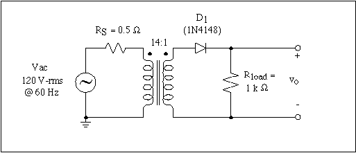
Fig. 3.16 Half-wave rectifier
circuit using a transformer with a 14:1 turns ratio to step down the line
voltage of 120 V-rms to 12 V-peak.
A half-wave rectifier circuit is shown in Fig. 3.16. It consists of a transformer
with a 14:1 turns ratio, a single diode D1 of the commercial type 1N4148,
and a load resistance Rload of 1 k Ohm. The source resistance of 0.5 Ohm
of the AC line is also included in this circuit. The purpose of the transformer
is to step down the main household AC power supply voltage of 120 V-rms
to a 12 V-peak level. Spice does not make provision for an ideal transformer,
probably for a good reason; one does not exist in practice. Instead, Spice
allows coupled inductors to be described having a coefficient of coupling
k less than one. Two inductors, say for example, LP and LS,
which share a common magnetic path and have a coefficient of coupling k
very close to unity, say 0.999, would be a reasonably good model of many
practical transformers. The turns ratio NP/NS of such a transformer is given
by the square-root of the ratio of the primary to secondary inductance,
ie. NP/NS = (LP/LS)^1/2.
To describe such a transformer to Spice, three element statements are required:
One statement for each inductor, and a statement that describes the coefficient
of coupling between the two inductors. Inductor coupling is described to
Spice using a new statement that begins with the letter K. If more than
two inductors share a common magnetic path, then a unique name is attached
to K to uniquely identify each coefficient of coupling. This is then followed
by the names of the two inductors that are magnetically coupled together.
These names must correspond with the names of two inductors described in
the present Spice deck. Subsequently, the final field of this statement
describes the coefficient of coupling k, which can take on a value
between 0 and 1. Since Spice does not accept a value of k equal to
unity, we shall always in this book use k=0.999. The transformer
``dot'' convention is adhered to in Spice. Observe that the ``dot'' of each
transformer is
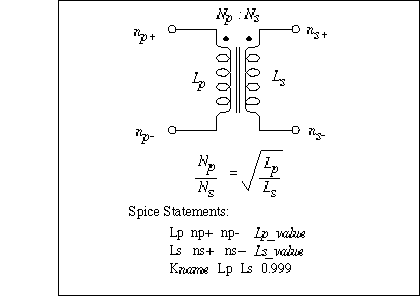
Fig. 3.17 The general syntax
of the Spice statements used to describe a (nonideal) transformer. The transformer
turns ratio NP:NS is determined by the appropriate selection of primary
and secondary inductor values, LP and LS, respectively.
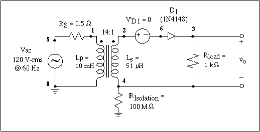
Fig. 3.18 Preparing the half-wave
rectifier circuit shown in Fig. 3.16 for Spice analysis: A large-valued
isolation resistor (100 M Ohm) is placed between the secondary side of the
transformer and ground. This provides a DC path between the secondary side
of the transformer and the common reference node (0). Also added is a zero-valued
voltage source in series with the rectifier diode. This will allow indirect
access to the diode current.
located at the positive node (n+) of each inductor. Extension to three or
more coupled inductors should be self-evident. N coupled inductors requires
N inductor element statements and N(N+1)/2 coefficient of coupling statements.
For a transformer consisting of two coupled coils, Fig. 3.17 illustrates
the three Spice statements necessary to describe it to Spice.
Half-Wave Rectifier Circuit
** Circuit Description **
* ac line voltage
Vac 5 0 sin (0 169V 60Hz)
Rs 5 1 0.5
* transformer section
Lp 1 0 10mH
Ls 2 4 51uH
Kxfrmr Lp Ls 0.999
* isolation resistor (allows secondary side to pseudo-float)
Risolation 4 0 100Meg
* diode current monitor
VD1 2 6 0
* rectifier circuit
D1 6 3 D1N4148
Rload 3 4 1kOhm
* diode model statement
.model D1N4148 D (Is=0.1pA Rs=16 CJO=2p Tt=12n Bv=100 Ibv=0.1p)
** Analysis Requests **
.TRAN 0.5ms 100ms 0ms 0.5ms
** Output Requests **
.plot TRAN V(3,4) V(2,4) V(1)
.plot TRAN V(6,3)
.plot TRAN I(VD1)
.probe
.end
Fig. 3.19 The Spice input file
for calculating the transient behavior of the half-wave rectifier circuit
shown in Fig. 3.18.
Returning to the half-wave rectifier circuit of Fig. 3.16 we can create
a Spice description of this circuit. We shall assume that the inductance
of the primary side of the transformer is 10 mH, and the inductance of secondary
side is 51 uH. This will provide an effective transformer turns ratio of
14:1. Continuing, the alert student will quickly realize that the circuit
on the secondary side of the transformer has no DC path to ground and will
therefore be rejected by Spice. To circumvent this situation, we simply
add a large resistor between ground and one point on the secondary side.
The value of this resistor should be chosen such that it does not significantly
interfere with the operation of the circuit. Fig. 3.18 illustrates the addition
of a 100 M Ohm between ground and node 4 of the rectifier. Also shown in
this figure is a zero-valued voltage source placed in series with the rectifier
diode D1. This will enable us to monitor the current flowing through the
diode. The resulting Spice deck for this modified circuit is seen listed
in Fig. 3.19. A transient analysis is requested to compute the voltage appearing
across the load resistance, the voltage appearing across the primary- and
secondary-side of the transformer, and finally, the AC line voltage. The
Spice model of the commercial diode, 1N4148, was obtained from a library
of Spice models for various electronic components included in PSpice.
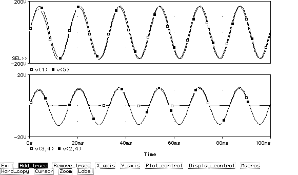
Fig. 3.20 Various voltage waveforms
associated with the half-wave rectifier circuit shown in Fig. 3.18. The
top graph displays both the AC line voltage and the voltage appearing across
the primary-side of the transformer. The bottom graph displays the voltage
appearing across the load resistor and the voltage appearing across the
secondary-side of the transformer.
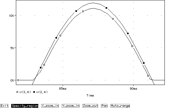
Fig. 3.21 Zooming-in on a half
cycle of the voltage waveform appearing across the load resistor and comparing
it to the voltage developed across the secondary-side of the transformer.
The results of the Spice analysis are shown in Fig. 3.20. The top graph
displays the voltage waveform of the AC line voltage (Vac) and the voltage
appearing across the primary-side of the transformer. Here we see that the
voltage across the transformer experiences a short transient effect, quickly
settling into its steady-state with the transformer voltage slightly lagging
behind the line voltage. The bottom graph displays the rectified voltage
appearing across the load resistance and the voltage appearing across the
secondary-side of the transformer. A blown-up view of a half period of the
rectified output voltage and the transformer secondary-side voltage is shown
in Fig. 3.21.
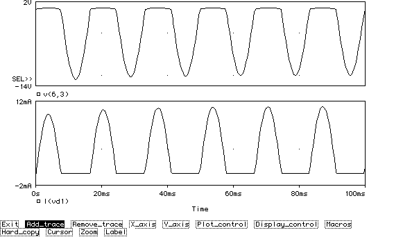
Fig. 3. 22 The voltage and
current waveform associated with diode $D_1$. The peak inverse voltage (PIV)
is seen to be 12 V and the maximum diode current is 11.1 mA.
An important consideration in the design of rectifier circuits is the diode
current-handling capability, determined by the largest current that it has
to conduct, and the peak inverse voltage (PIV) that the diode must be able
to withstand without breakdown. In Fig. 3.22 we display both the voltage
across the diode and the current that it conducts. We see that the PIV of
this particular rectifier circuit is 12 V. Because the diode has not broken
down, we can assume that the breakdown voltage of the 1N4148 commercial
diode is larger than 12 V. In fact, data sheets of the 1N4148 diode indicate
that its breakdown voltage is in the vicinity of 100 V. The maximum current
that the diode has to conduct is seen to be about 11 mA. Using the cursor
facility of Probe, we find that it is 11.1 mA. The data sheets of the 1N4148
indicate that this diode can handle a peak current of no more than 100 mA,
thus our rectifier design is well within the limits of the 1N4148.